01
Requirement Clarification
We start with the target wavelength, output power, operation mode, package form, optical path, working distance, spot size and application direction.
DEVELOPMENT PROCESS
Custom laser source projects usually start from wavelength, output power, operating mode, package preference, optical layout and application environment. We help define the suitable VCSEL, selected EEL, package, optical or module-level path before moving forward.
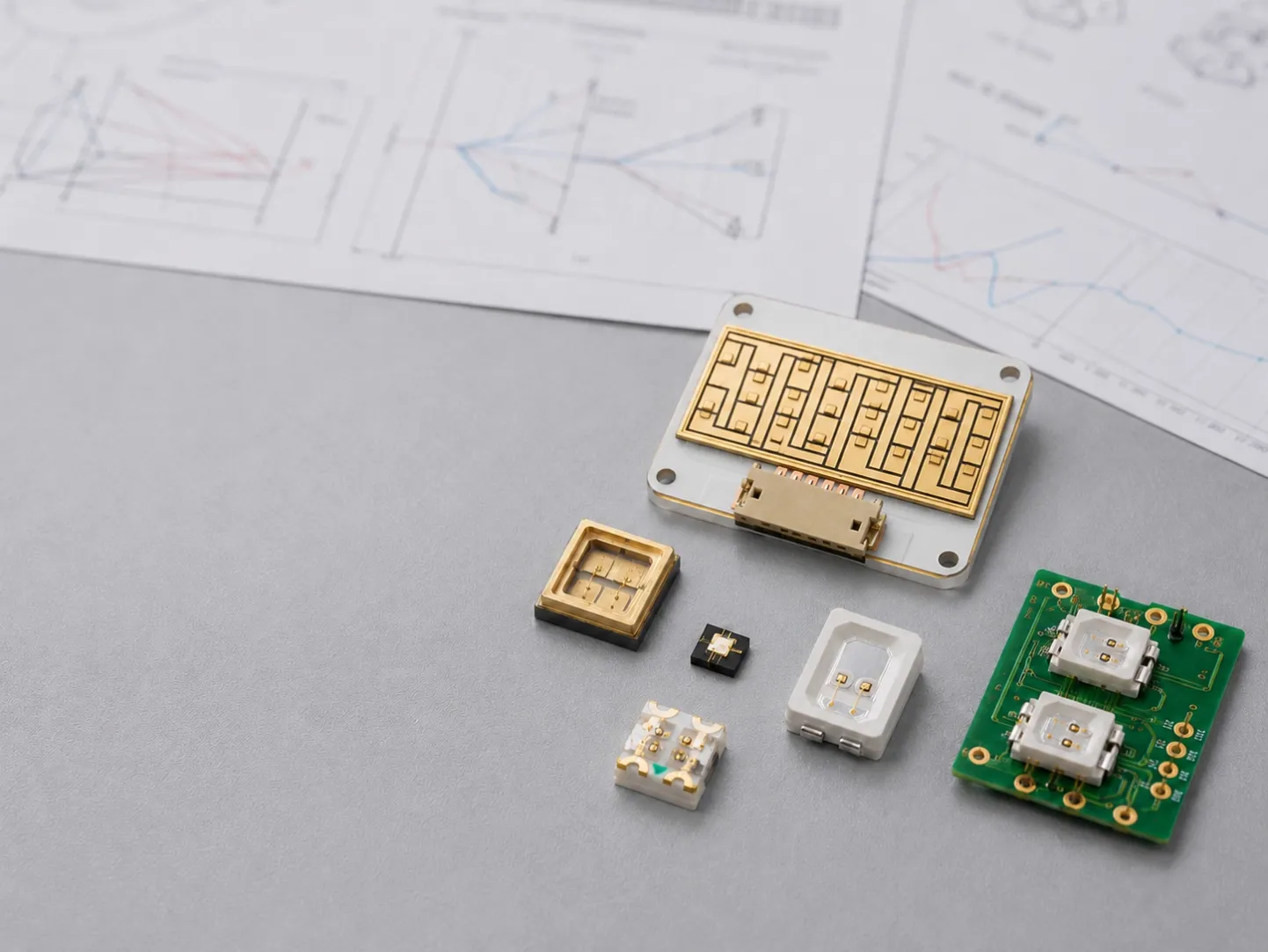
The process is designed for custom VCSEL wafer-level development, VCSEL array projects, package customization, COB assemblies, optical module integration and selected EEL or pump laser module discussions.
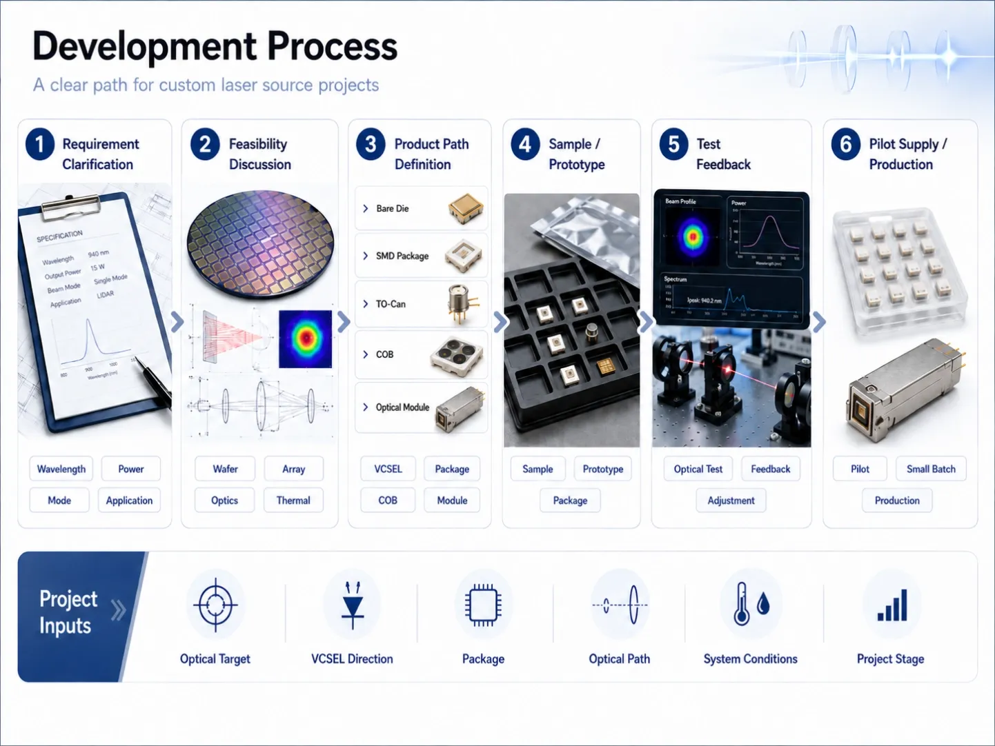
PROJECT FLOW
Each custom project follows a practical engineering path, from requirement clarification to product path definition, sample preparation, test feedback and pilot supply discussion.
We start with the target wavelength, output power, operation mode, package form, optical path, working distance, spot size and application direction.
The requirement is discussed from VCSEL wafer-level design, array layout, package path, thermal condition, optics and module integration.
We confirm whether the project should follow a standard product, modified package, VCSEL array, COB assembly, optical module or selected EEL path.
Samples or prototypes can be arranged based on product availability, custom scope, package form, test needs and project stage.
Customer test data can help adjust wavelength target, optical output, beam behavior, package details, array layout or module-level design direction.
After key parameters are confirmed, the project can move toward pilot supply, small-batch delivery or custom production discussion.
PROJECT INPUTS
Clear input information helps shorten communication time and define the suitable wafer-level, package, optical or module-level development path.
Please provide the target wavelength, optical output power, tolerance range and whether the source should operate in CW, QCW or pulse mode.
Please specify whether the project needs single-mode, multi-mode, VCSEL array, 1D / 1.5D / 2D layout, emitter count, pitch or addressing.
Please share the preferred package path, such as bare die, SMD, TO-CAN, TO-46, TO-52, TO-56, COB, ceramic submount or module structure.
Please provide working distance, target spot size, beam angle, collimation needs, diffuser requirements and any coupling optics constraints.
Please provide drive current, voltage range, duty cycle, pulse condition, heat dissipation method and expected operating temperature.
Please describe the application direction, target product, current project stage, expected quantity and whether the request is for evaluation, prototype or pilot supply.
NEXT STEP
Send us your target wavelength, output power, operation mode, array layout, package preference, collimation or diffuser needs, working distance, spot size and application direction. We will check the suitable wafer-level, package, optical or module path.