CUSTOM DEVELOPMENT

Custom Laser Source Development from Wafer-Level Design to Module Integration.

We support custom optical source discussions from VCSEL wafer-level design, wavelength and output power definition, operating mode, array structure, package path, COB assembly, beam collimation, diffuser customization, coupling optics and module-level laser source integration.

VCSEL is our main product direction, covering standard wavelength directions from 650nm to 1064nm, with additional custom wavelength discussions available by project. Supported directions include single-mode VCSEL, multi-mode VCSEL, VCSEL array, CW / QCW / pulse operation, and selected discussions.

Custom laser source development image showing VCSEL wafer, FR4 PCB, optical components, and module integration workflow for VCSEL source projects.
Custom laser source development from VCSEL wafer-level design to package, optics and module-level integration.

CUSTOMIZATION SCOPE

What Can Be Customized.

Custom laser source development from VCSEL wafer-level design to package, optics and module-level integration.

Wafer-Level Design1

Wafer-Level VCSEL Design and Wavelength

Custom requirements can be discussed from the VCSEL wafer-level design stage, including standard wavelength directions from 650nm to 1064nm, project-specific custom wavelengths and optical output power targets.

650NM–1064NM / CUSTOM WAVELENGTH / OUTPUT POWER
Mode and Operation2

Single-Mode, Multi-Mode and Operation Mode

Single-mode and multi-mode VCSEL directions can be discussed together with CW, QCW and pulse operation. Single-mode is suitable for atomic clocks, OPM magnetometers and precision optical sources, while multi-mode supports higher-power sensing, medical beauty and module-level source projects.

SINGLE-MODE / MULTI-MODE / CW-QCW-PULSE
VCSEL Array3

VCSEL Array and Emitter Layout

VCSEL array is a key customization direction. We can discuss emitter count, pitch, electrode routing, addressing method, target spot distribution, and 1D / 1.5D / 2D array layouts for sensing, structured light and high-NRE array projects.

1D / 1.5D / 2D ARRAY / EMITTER LAYOUT
Package Path4

Package and Material Options

Package paths can be customized around SMD, TO-CAN, COB, ceramic submounts and module-level structures. SMD support materials may include PCT, aluminum nitride, alumina and transparent resin carriers. TO package discussions can include TO-46, TO-52 and TO-56 copper-can structures.

SMD / TO-CAN / COB / CERAMIC SUBMOUNT
Multi-Wavelength5

Multi-Wavelength Package Integration

For multi-wavelength source platforms, integrated package discussions can support up to 6-in-1 wavelength combinations for medical beauty, phototherapy, multi-channel sensing, combined-wavelength sources and OEM platform development.

UP TO 6-IN-1 / MULTI-WAVELENGTH / OEM PLATFORM
Module and EEL6

COB, Optical Module and EEL Pump Source

COB source assemblies, high-power NIR modules, thermal path design, beam collimation, diffuser customization, coupling optics and module-level integration can be discussed. Selected EEL, Laser Stack and Nd:YAG pump modules are also available by project.

COB / COLLIMATION / DIFFUSER / EEL PUMP SOURCE

VCSEL ARRAY CAPABILITY

Wafer-Level VCSEL and Array Customization Data.

This section highlights VCSEL wafer-level customization and array development targets, including emission aperture, array layout, spectral consistency, power uniformity and operation mode. Final targets depend on wavelength, epitaxial structure, emitter count, layout, drive mode and package path.

01

4.5–6μm Emission Aperture Design

VCSEL emission aperture can be discussed by project. Typical array designs may use 5.5–6μm apertures, while minimum aperture direction can reach around 4.5μm for compact, high-density array development.

02

1D / 1.5D / 2D VCSEL Array Layout

VCSEL arrays can be discussed in 1D, 1.5D or 2D emitter layouts, including emitter count, pitch, row arrangement, electrode routing, addressing method and target spot distribution.

03

≤0.5nm Spectral Consistency Target

For selected custom array projects, spectral consistency can be discussed as a key development target, with ≤0.5nm direction for applications requiring multi-emitter wavelength matching.

04

≤10% Power Uniformity Target

Array power uniformity can be discussed according to customer requirements, with ≤10% target direction for sensing arrays, multi-point source designs and high-consistency array projects.

05

CW / QCW / Pulse Operation

CW, QCW and pulse operation can be discussed according to thermal design, peak power, average power, drive condition, package path and system-level operating mode.

06

NRE-Based Array Development

For array needs beyond standard products, NRE development can cover wafer-level design, emitter layout, aperture size, pitch, electrode routing, uniformity target and prototype iteration.

OPTICAL & MODULE DATA

Optical Integration Data for Custom Source Projects.

Custom laser source projects may require package design, thermal path, beam collimation, diffuser customization, coupling optics, beam uniformity and module-level optical integration. Wafer-level optical resources can support micro-optics, lens arrays, gratings and silicon lens discussions.

01

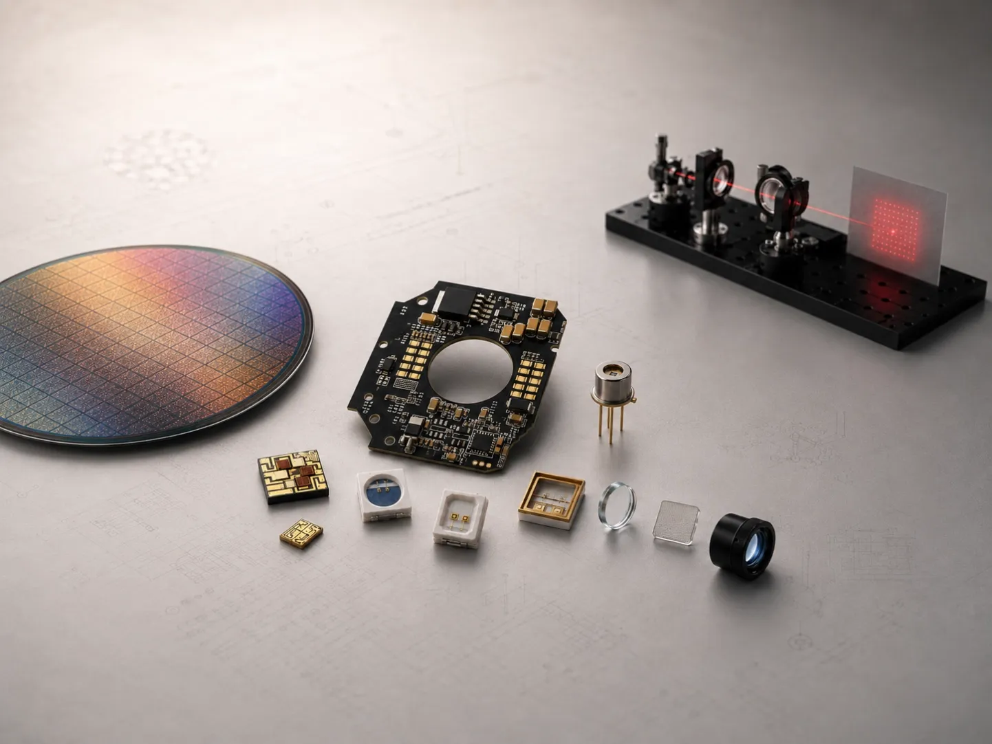
2–8 Inch Wafer-Level Optical Resources

Wafer-level optical resources can support 2–8 inch optical microstructure processes, including lithography, nanoimprint, etching, coating-related process discussion and 3D profile measurement.

02

±1μm Wafer Alignment Accuracy

Reference optical process data includes 8 inch wafer alignment accuracy of ±1μm, supporting discussions around MLA, silicon lens arrays, coupling optics and microstructure alignment.

03

±0.4% Profile Uniformity

Surface profile uniformity can be controlled toward ±0.4%, supporting micro-lens arrays, silicon lenses, coupling lenses and other wafer-level optical component discussions.

04

φ5–900μm Silicon / Quartz Lens Options

Silicon and quartz lens resources can cover φ5–900μm lens diameters for VCSEL collimation, coupling optics, silicon lens arrays and compact optical source designs.

05

RMS <25nm Surface Profile Error

Silicon lens reference data includes surface profile error below 25nm RMS, supporting high-precision coupling lenses, collimation lenses, lens arrays and micro-optical components.

06

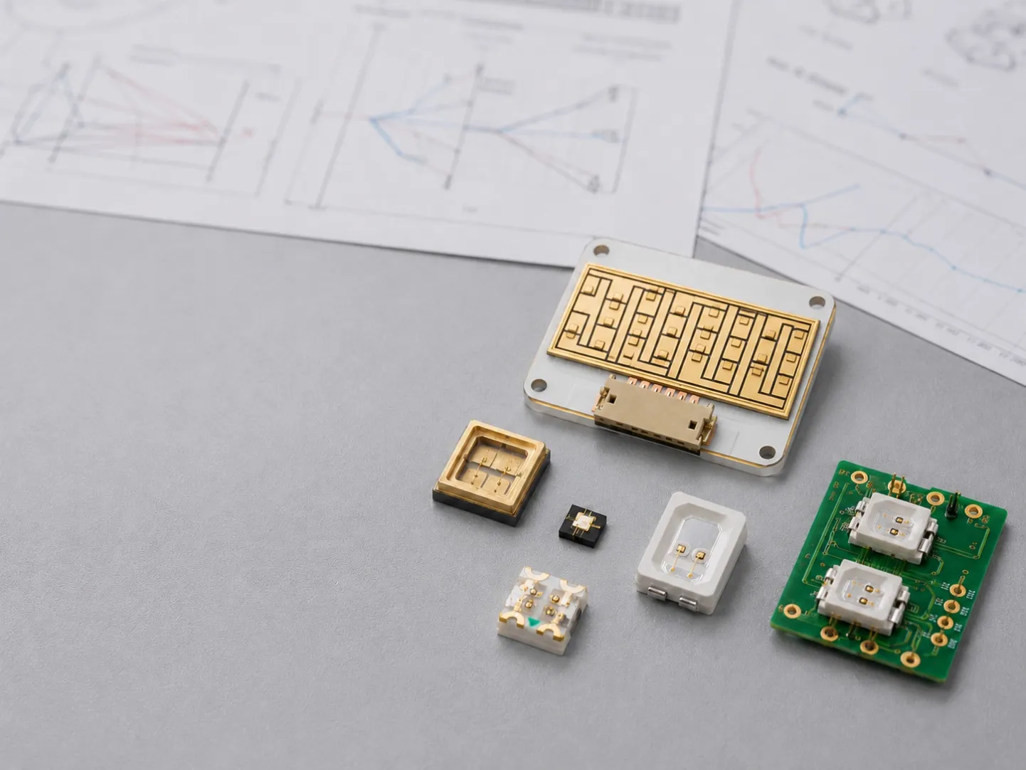
Collimation, Diffuser and Coupling

Optical design discussions can include VCSEL collimation, diffuser customization, coupling optics, MLA, silicon lens arrays, custom spot size, beam uniformity and module-level optical path integration.

NEXT STEP

Ready for the Next Step?

Send us your target wavelength, output power, operation mode, array layout, package preference, collimation or diffuser needs, working distance, spot size and application direction. We will check the suitable wafer-level, package, optical or module path.

VCSEL and laser source components for custom optical source development