
650nm
650nm 5mW VCSEL SMD Series
650nm 5mW VCSEL SMD series with a Annular beam spot and 1615–5050 package options for hair-growth, red-light therapy and PCB integration.
Specifications
- Wavelength
- 650nm typ.
- Optical Output Power
- 5.5mW typ.
- Operating Mode
- CW
- Test Current
- 10mA
- Forward Voltage
- 2.4V typ.
- Beam Divergence
- 25° typ.
- Beam Profile
- Annular beam spot
- SMD Package Options
- 1615 / 2835 / 3030 / 3535 / 5050
Product Overview
1. Standard 650nm 5mW VCSEL SMD Series
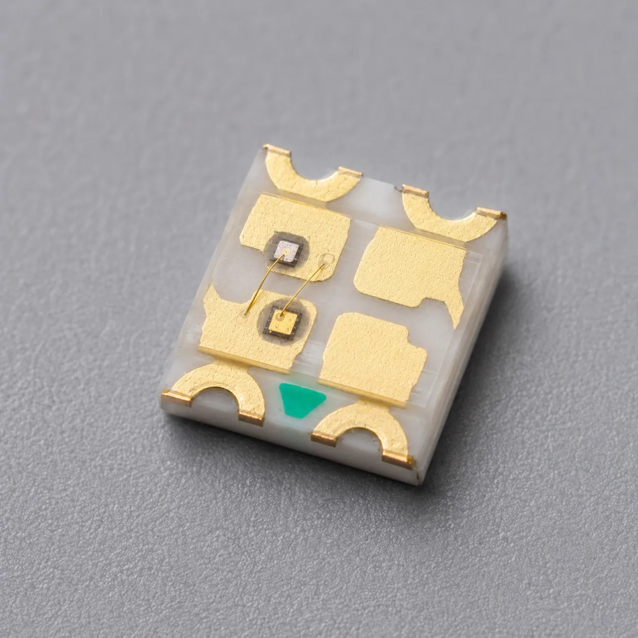
The 650nm 5mW VCSEL SMD Series is a visible-red surface-mount laser device suitable for direct mounting onto printed circuit boards through standard SMT processes and for further integration into optical assemblies and finished optoelectronic products.
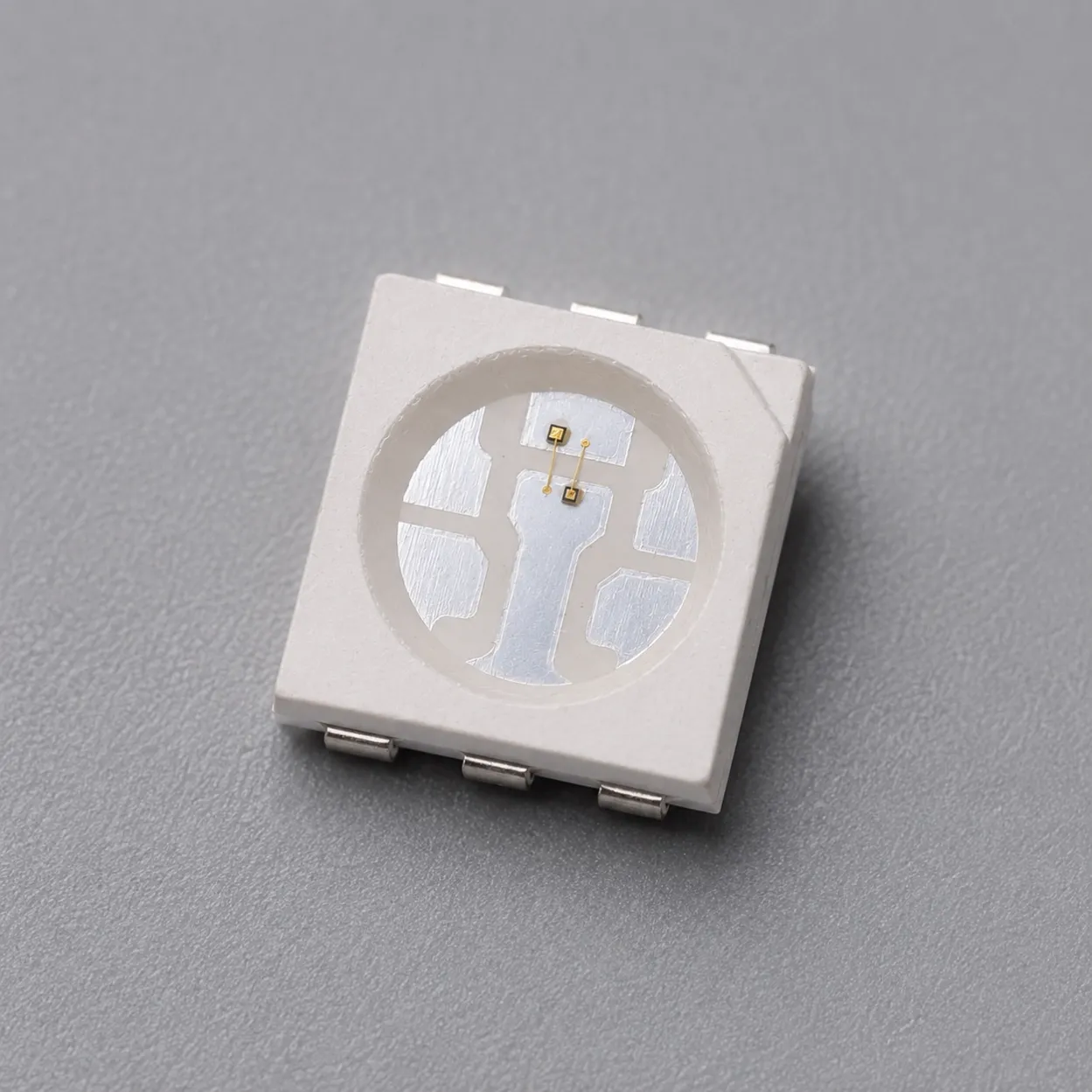
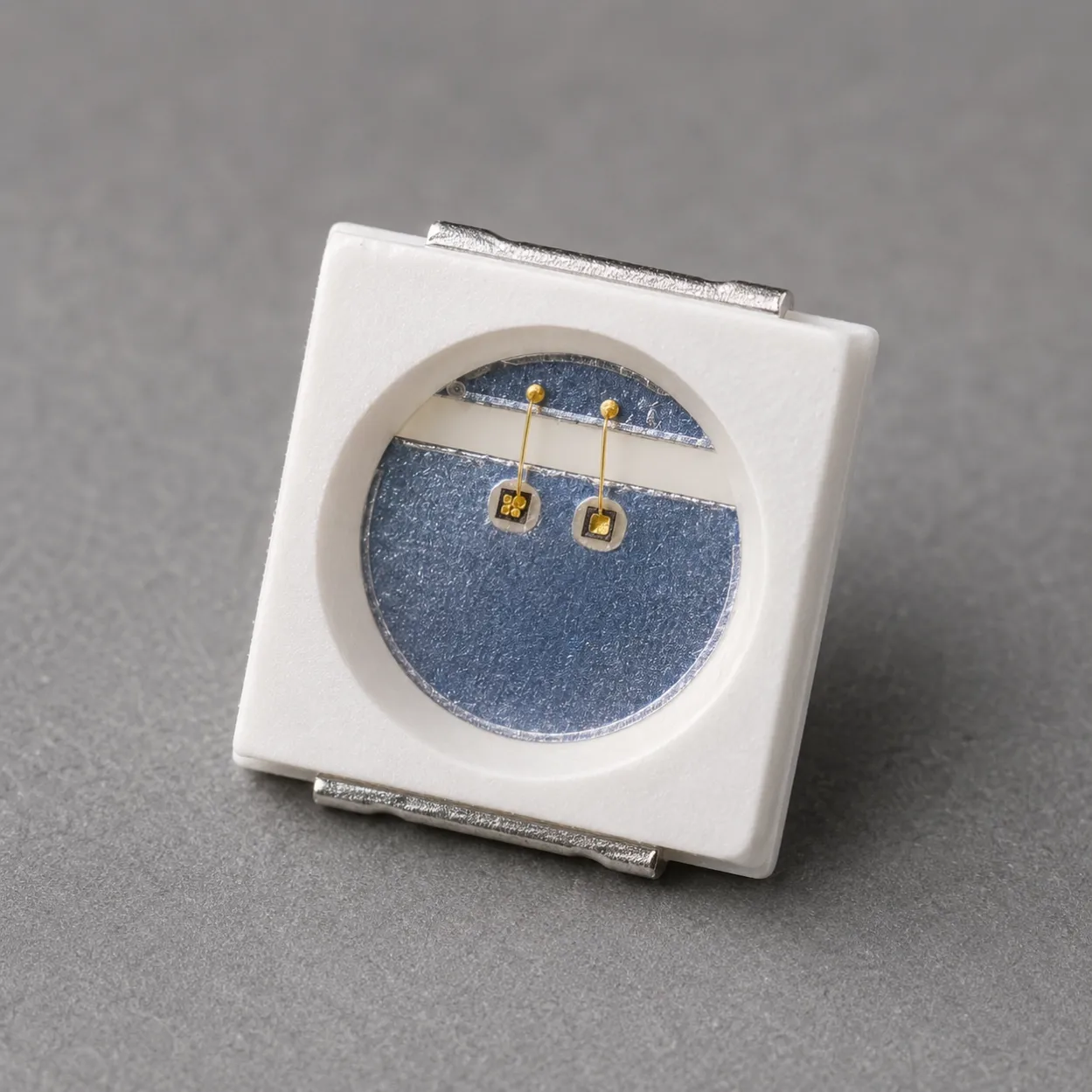
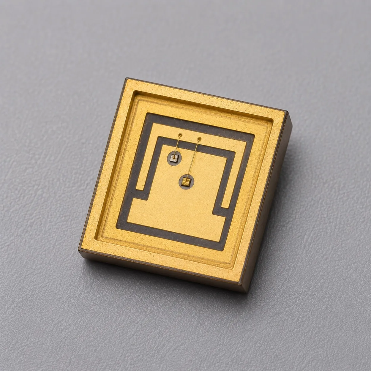
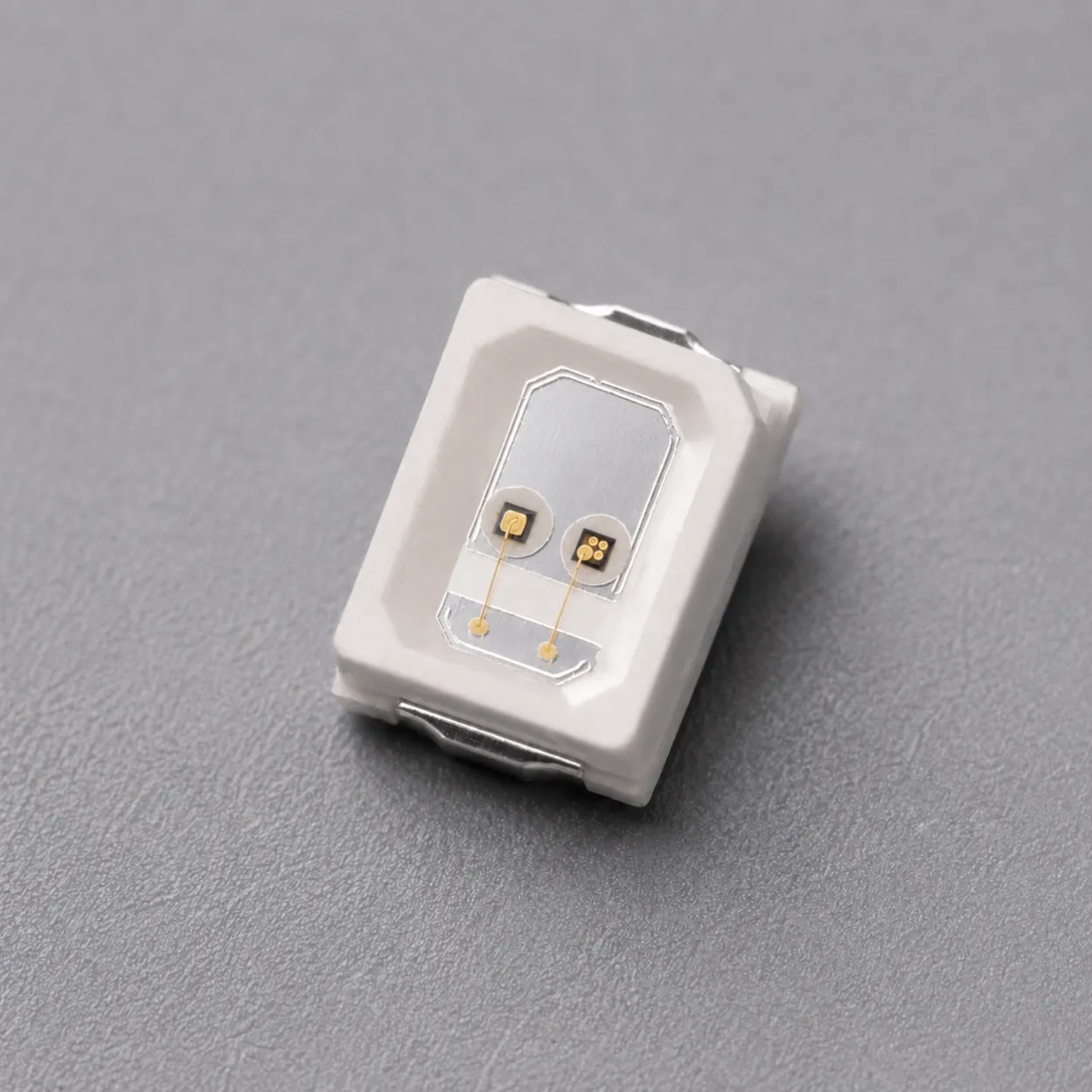
The series is available in five SMD package formats: 1615, 2835, 3030, 3535 and 5050. The 1615, 2835, 3030 and 5050 versions use PCT support structures, while the 3535 version uses a ceramic support structure. Customers can select the appropriate package according to PCB space, pad layout, component height, optical opening and product enclosure design.
Package | Material | Size | Selection Guide |
|---|---|---|---|
1615 | PCT | 1.6 × 1.5mm | Compact, low-profile designs |
2835 | PCT | 3.5 × 2.8mm | Rectangular SMT layouts |
3030 | PCT | Approx. 3.18 × 3.0mm | Compact square layouts |
3535 | Ceramic | 3.5 × 3.5mm | Ceramic package requirements |
5050 | PCT | 5.0 × 5.0mm | Larger spacing or optical openings |
All five standard package formats use a 7mil × 7mil VCSEL chip and provide consistent core optical and electrical performance. Customers can therefore select different package formats according to the mechanical structure and PCB design of the finished product while maintaining the specified 650nm light-source characteristics.
The series produces an annular, donut-shaped beam spot. Compared with conventional TO-can through-hole packages, the SMD formats are better suited to direct PCB mounting, low-profile product structures and distributed multi-emitter layouts.
In addition to the standard 1615, 2835, 3030, 3535 and 5050 formats, other SMD package sizes, support materials or pad configurations can also be discussed according to the specific product design. Please Contact Us to provide your package requirements.
2. Detailed Optical and Electrical Characteristics
The Specifications section at the top of the page presents the primary product-selection parameters. The following table provides the minimum, typical and maximum values required for component evaluation and product development.
Parameter | Min. | Typ. | Max. | Condition |
|---|---|---|---|---|
Wavelength | 640nm | 650nm | 660nm | CW |
Output Power | 5.0mW | 5.5mW | 7.2mW | IF = 10mA |
Threshold Current | — | 4mA | — | CW |
Series Resistance | — | 48Ω | — | CW |
Slope Efficiency | — | 0.6W/A | — | CW |
Wavelength Shift | — | 0.047nm/°C | — | Temperature |
Chip Size | — | 7mil × 7mil | — | — |
The five standard package formats provide consistent core optoelectronic performance. Their main differences are package dimensions, support materials, pad structures and required mounting space. Detailed mechanical dimensions, polarity information and reflow soldering profiles are provided in the corresponding package datasheets.
3. Replacing Conventional 650nm TO-can Through-Hole Packages
This SMD series is particularly suitable for upgrading products that currently use conventional 650nm TO-can through-hole devices to automated surface-mount assembly.
Compared with through-hole packages, the SMD structure can reduce component height and eliminate several manual production steps, including component insertion, lead trimming and secondary soldering. It also supports more compact PCB, optical and mechanical layouts.
The available packages are compatible with conventional pick-and-place equipment and standard SMT production processes. This can help reduce assembly and processing costs, improve manufacturing consistency and product yield, and shorten volume-production time.
Multiple package sizes also provide greater design flexibility for arranging emitter spacing, PCB dimensions, optical openings and product enclosure structures.
4. Hair-Growth, Beauty and Red-Light Applications
The 650nm visible-red wavelength, 5mW-class optical output and annular beam spot make this series suitable for compact red-light equipment, wearable products and handheld beauty-care devices.
Key development directions include hair-growth caps, hair-growth helmets, hair-growth combs, hair-growth bands, beauty pens, red-light therapy products, personal-care equipment and other integrated visible-red optoelectronic systems.
For hair-growth, beauty-care and red-light product development, the device can be used as a component-level 650nm light source. It can be integrated as a single emitter or arranged as multiple SMD emitters distributed across a PCB to accommodate different product shapes, emitter densities and illumination-area layouts.
The annular beam spot can be considered together with emitter spacing, array arrangement and the optical structure of the finished product. The low-profile SMD structure is also suitable for curved wearable products and compact handheld devices such as beauty pens and hair-growth combs.
If the standard configuration does not fully meet the project requirements, custom center wavelength, wavelength tolerance, optical output power, power-bin selection, package dimensions, support materials, optical structures and product-level integration solutions can also be discussed. Please use Submit Custom Development & ODM to provide the detailed technical requirements.
5. Evaluation Kit and Documentation Support
Evaluation sample kits are available with 10 pcs / KIT. International express shipping costs are calculated according to the destination. Please use Submit Your Evaluation Kits to submit the sample request and project information.
The evaluation kit can support package selection, PCB pad verification, pick-and-place compatibility, drive-condition testing, annular beam-spot evaluation and product-structure validation. The 1615, 2835, 3030, 3535 or 5050 package can be selected according to product availability and project requirements.
For component-level project evaluation, an Initial Product Report for the 650nm 5mW VCSEL SMD Series has been filed with the U.S. FDA CDRH. This filing supports technical documentation and product evaluation.
CE-related documentation is also available for project evaluation, including EMC documentation and EN 60825 laser safety / LVD test documentation. Material compliance documentation, including RoHS, REACH and HF documentation, can also be provided according to project requirements.