01
Standard VCSEL Products
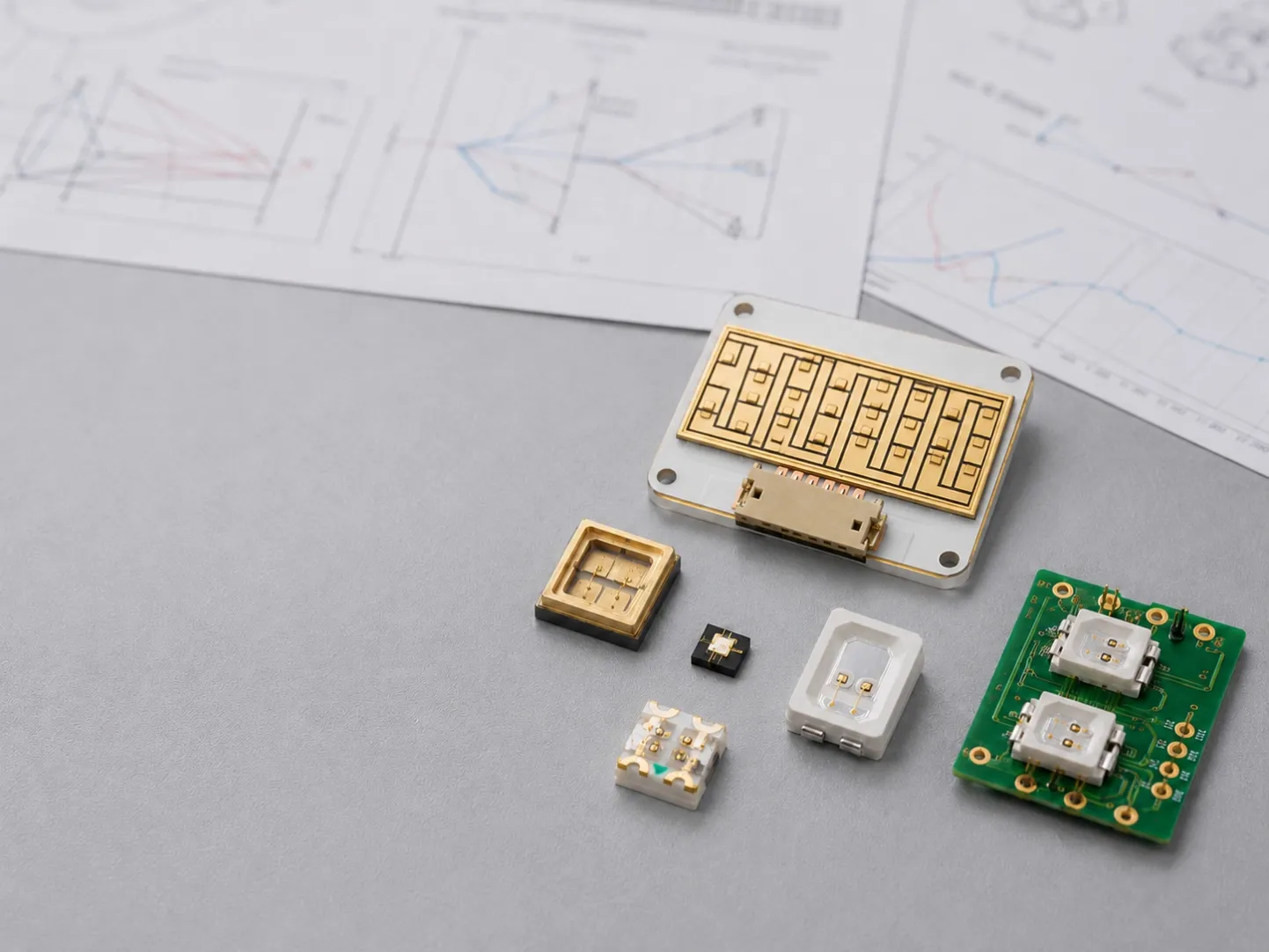
Standard VCSEL bare die, SMD, TO-CAN and COB product options for early evaluation, sample testing and wavelength-based product selection.
TECHNOLOGY PLATFORMS
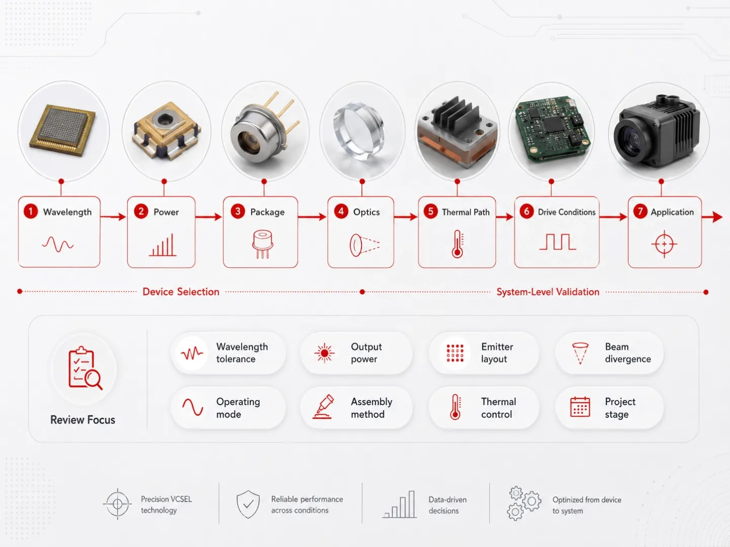
1ONELASER supports VCSEL product evaluation and development across standard products, chip-level customization, package design, MLA optics, wafer-level optical structures and VCSEL array integration discussions.
Our technology support is built around practical engineering needs, including wavelength selection, output power, emitter configuration, package type, beam control, thermal path, assembly method, documentation requirements and final application environment.
WHAT WE SUPPORT
We support customers from standard VCSEL product evaluation to chip-level customization, package development, MLA beam control, wafer-level optics, nanoimprint-related optical structures and VCSEL array integration discussions.
Standard VCSEL bare die, SMD, TO-CAN and COB product options for early evaluation, sample testing and wavelength-based product selection.
Chip-level discussions can cover wavelength, output power, emitter configuration, aperture layout, operating mode and project-specific optical requirements.
Package-level review may include ceramic submounts, wire bonding, thermal path design, package structure, assembly method and application-specific integration.
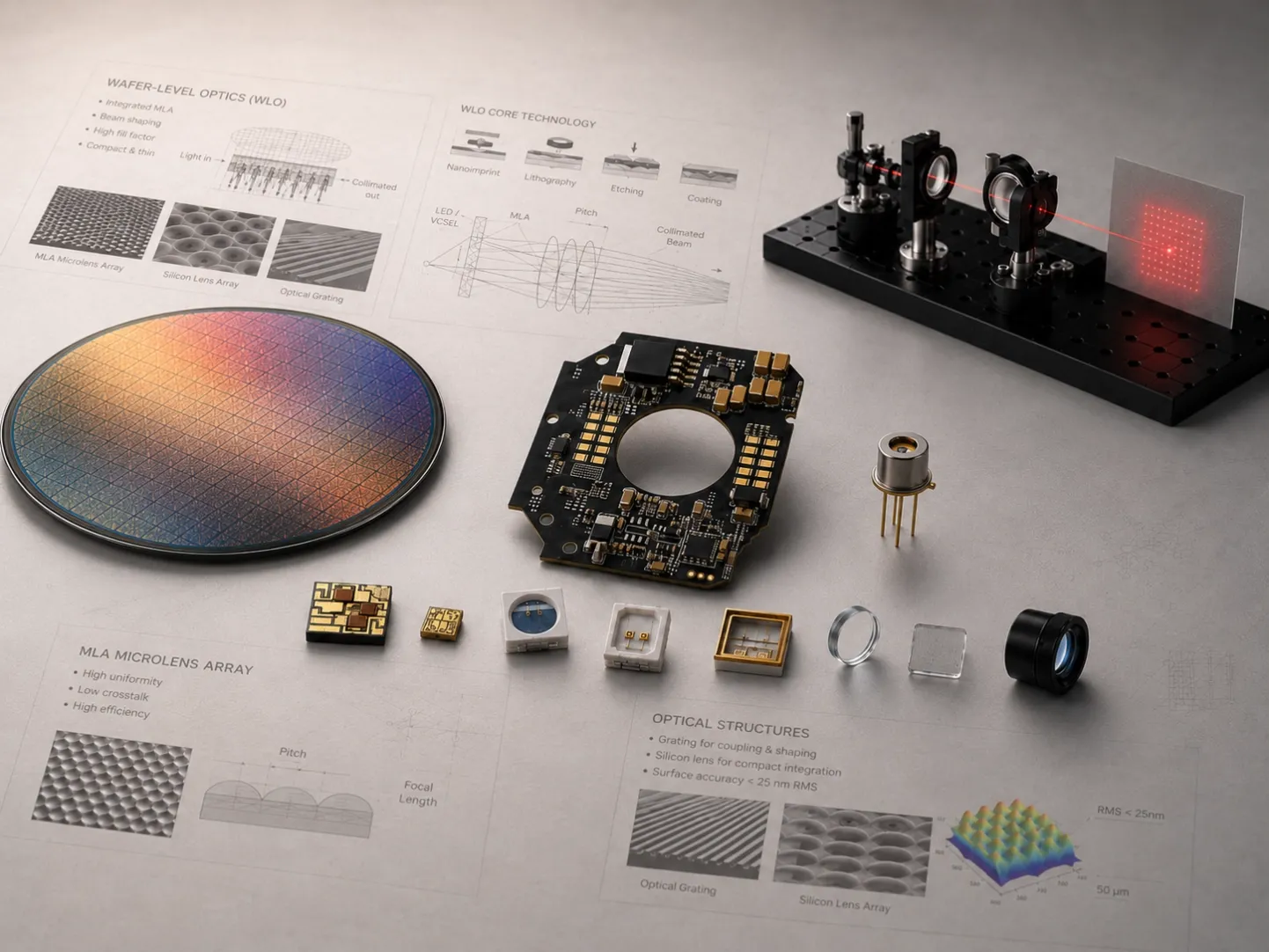
MLA optics, VCSEL collimation, beam shaping, divergence control, beam uniformity and optical alignment can be reviewed for application-specific beam profiles.
Wafer-level optics and nanoimprint-related structures are relevant to micro-lens arrays, gratings, silicon lenses, beam collimation and compact optical integration.
VCSEL array design, emitter layout, beam uniformity, thermal management, MLA optics and package-level optical source integration can be reviewed for selected projects.
ENGINEERING AND MANUFACTURING RESOURCES
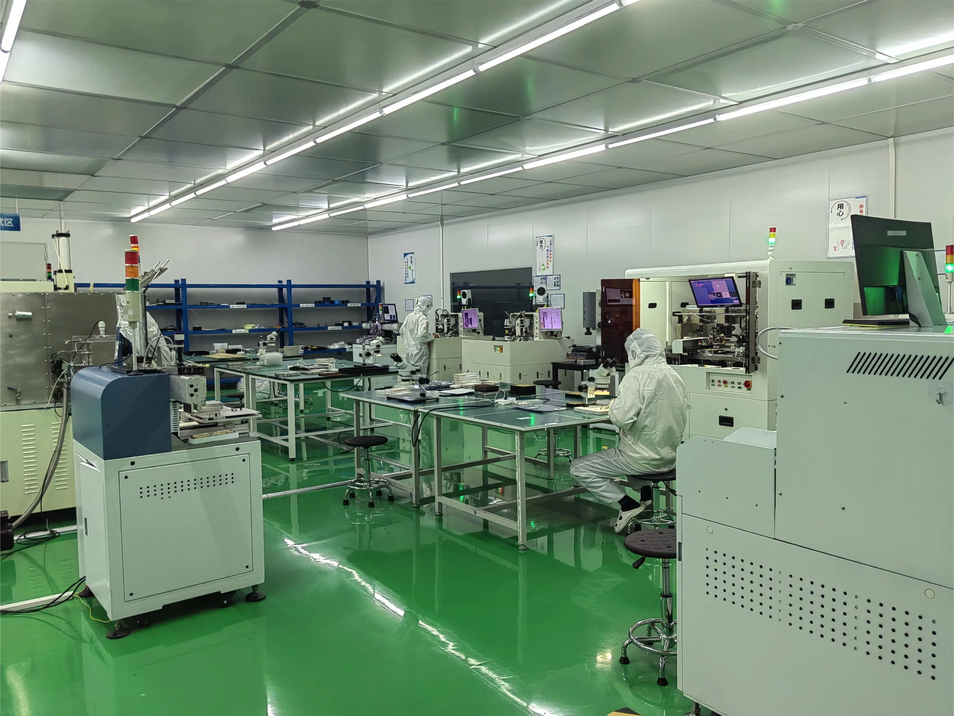
1ONELASER works with established wafer, packaging, assembly, optical, and module manufacturing resources to support standard VCSEL products, customized devices, evaluation samples, and OEM project delivery.
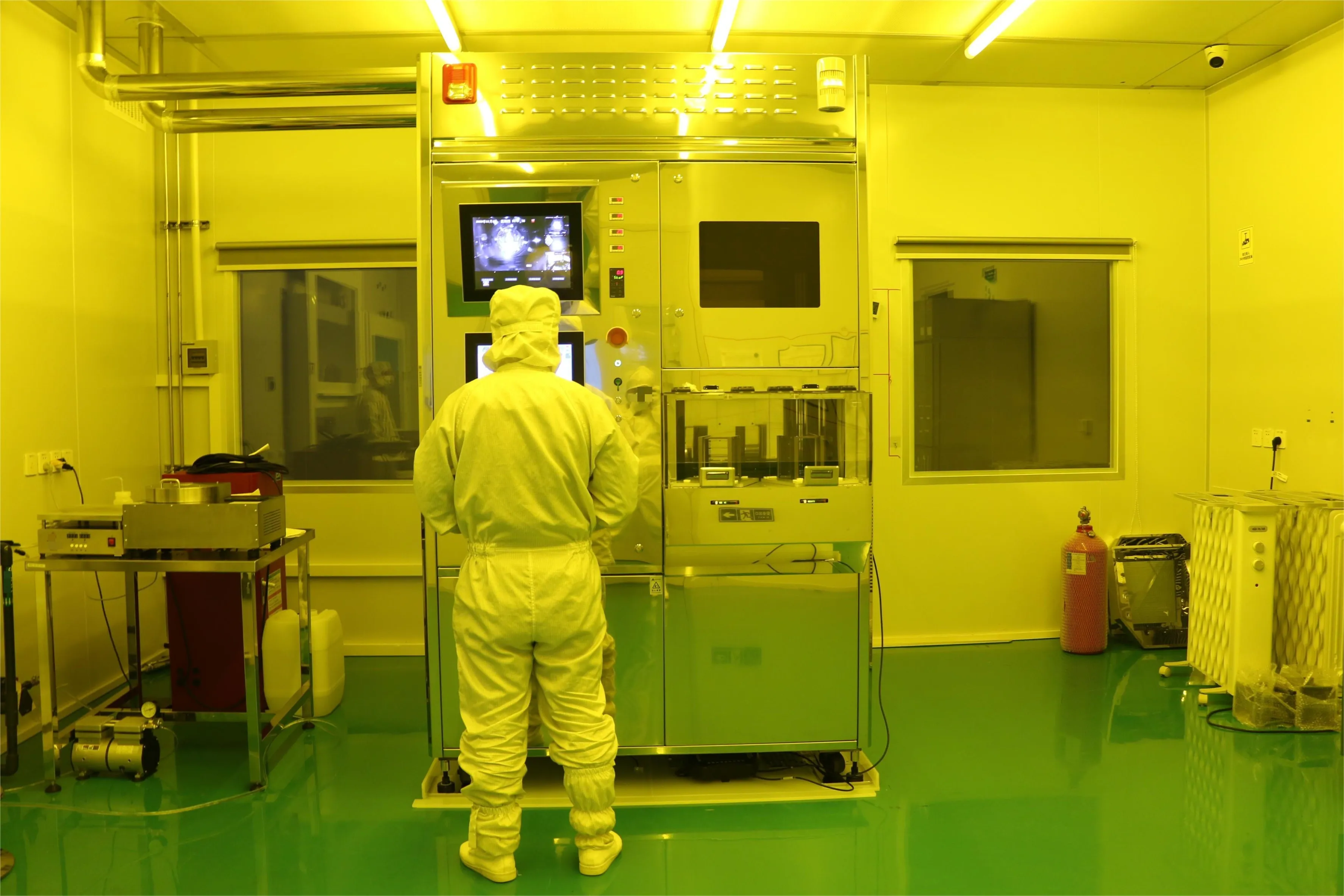
Wafer-level process resources can be reviewed for selected VCSEL development projects, including wavelength, aperture layout, optical structure, and process-related requirements.
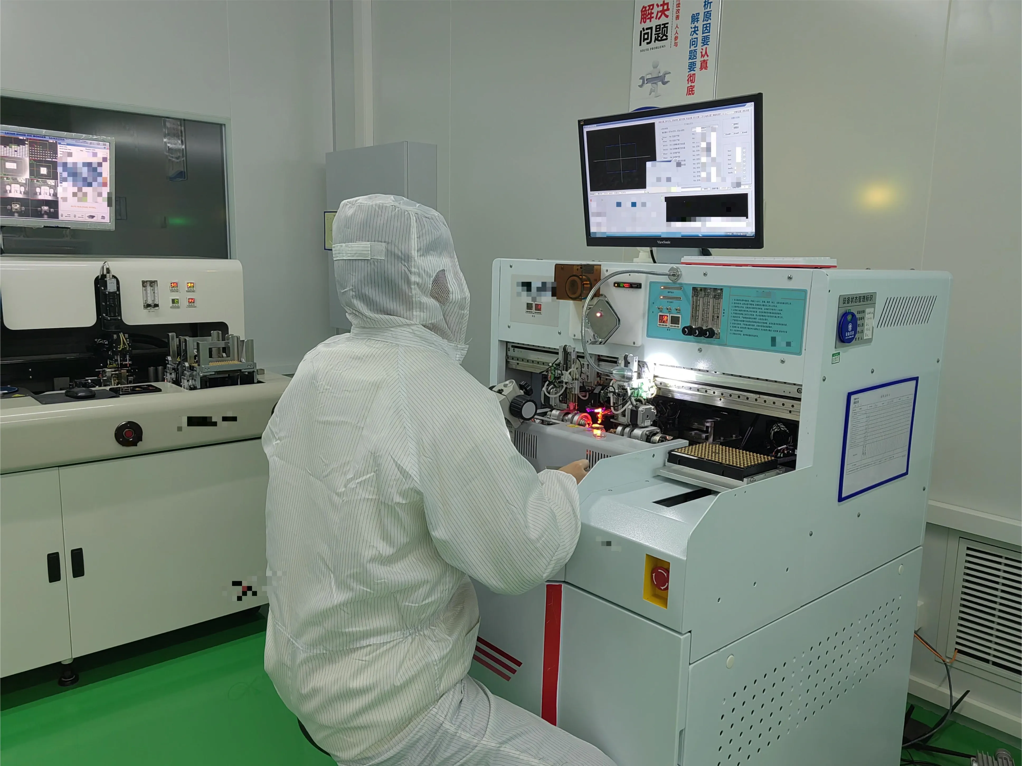
Packaging and assembly resources may support SMD, TO-CAN, COB, ceramic submount, wire bonding, thermal path review, and application-specific integration.
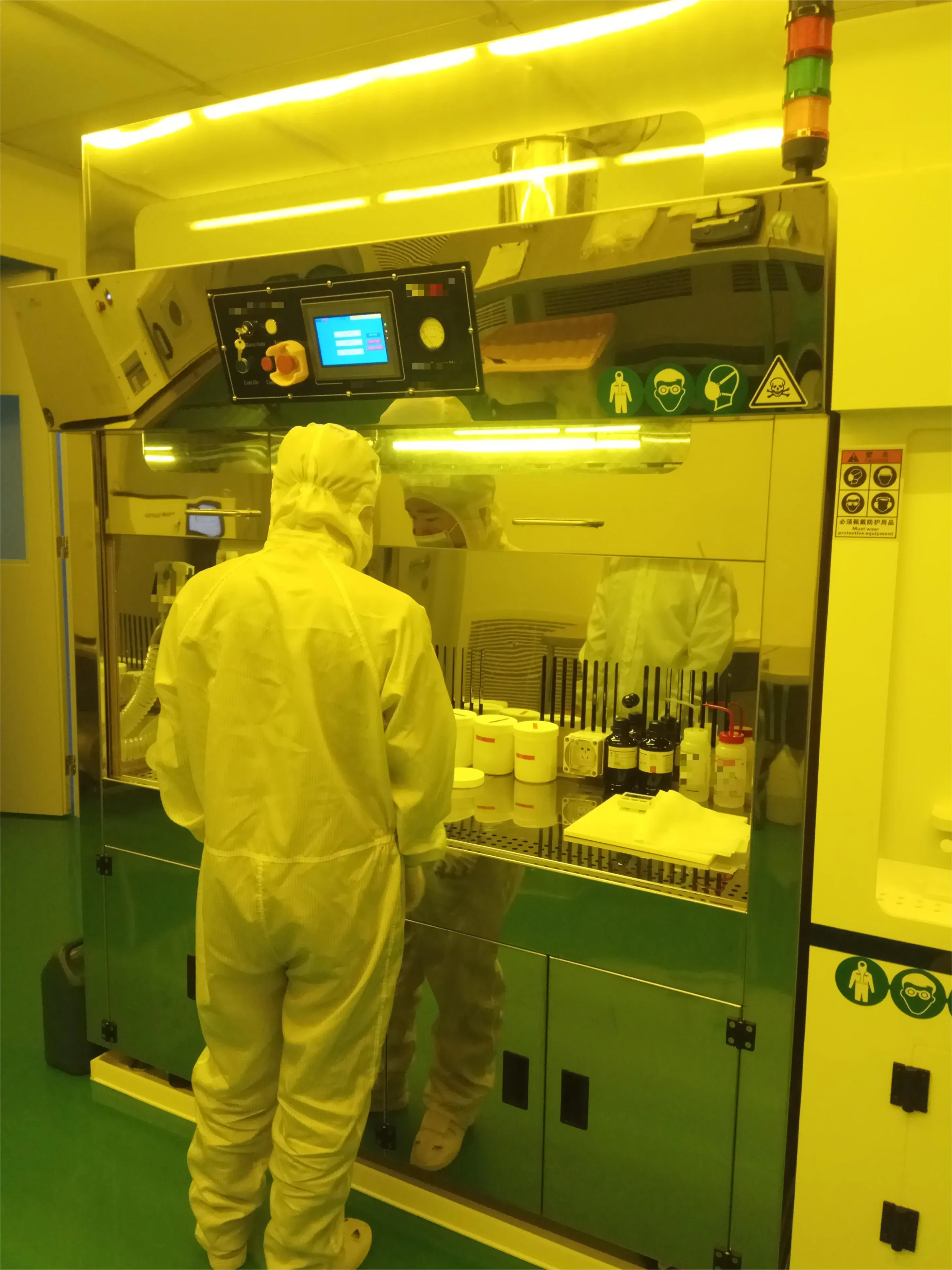
Inspection and testing resources can support sample review, optical structure inspection, output power check, beam profile review, and engineering feedback.
For selected OEM and custom development projects, sample preparation, manufacturing coordination, testing review, and delivery planning can be arranged based on project requirements.
ENGINEERING REVIEW
VCSEL selection is not only about wavelength or output power. The device should be reviewed together with package structure, thermal path, optical layout, drive conditions, documentation needs and final application environment.
We help customers review VCSEL options based on wavelength tolerance, output power, emitter layout, beam divergence, operating mode, assembly method, thermal control and project stage.
NEXT STEP
Send us your target wavelength, output power, operation mode, array layout, package preference, collimation or diffuser needs, working distance, spot size and application direction. We will check the suitable wafer-level, package, optical or module path.