
Oct 6, 2026Technical Insights
650nm VCSEL SMDs for Lighter, Thinner Hair-Growth Devices
650nm VCSEL SMDs replace TO-5.6 lasers with lower-current SMT packages, Zener protection, and PCB or FPC integration for hair-growth devices.
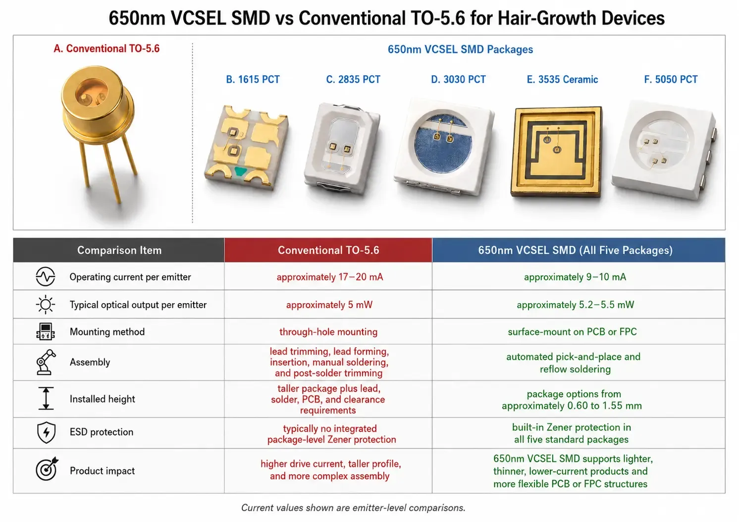
When engineering teams design a laser hair-growth cap or helmet, they usually begin with wavelength, optical power per emitter, and total laser count.
Package architecture often receives serious attention only after mechanical design, prototyping, or pilot production begins.
A single TO-5.6 laser diode is not exceptionally heavy or tall. The problem is that a hair-growth device rarely uses only one laser. It may contain 100, 200, or more than 300 emitters.
At that scale, the weight, height, current requirement, and assembly method of each component become system-level concerns.
A conventional 650nm TO-5.6 laser can deliver approximately 5mW of optical power, but it typically requires about 17–20mA of operating current. Production also commonly involves lead trimming, lead forming, through-hole insertion, manual soldering, and another trimming step after soldering.
These devices can be surface-mounted directly on a PCB or FPC, assembled through automated placement and reflow soldering, and operated at approximately 9–10mA to produce around 5.2–5.5mW of optical power.
For manufacturers still using TO-5.6 lasers, this is more than a package change.
It is an upgrade to a lighter, thinner, lower-current optical platform that is better suited to scalable SMT manufacturing.
1. Why TO-5.6 Limitations Grow With Larger Laser Arrays
A product containing only a few lasers may be able to absorb the weight and space requirements of TO-5.6 packages.
As the emitter count increases, however, those differences become much harder to ignore.
Package Weight Is No Longer a Small Number at 100 to 400 Emitters
A conventional TO-5.6 laser includes a metal housing, metal header, and long leads.
A compact SMD package eliminates the metal can and through-hole leads, so its individual package weight can be substantially lower.
Using published package-reference values, a TO-56 laser package may weigh approximately 0.3g, while a compact SMD laser package can weigh as little as approximately 0.027g.
That creates an estimated difference of about 0.273g per emitter.
The difference looks small at the component level. Across a complete array, it becomes much more significant:
Number of Lasers | TO-56 Weight at 0.3g Each | Compact SMD Weight at 0.027g Each | Estimated Weight Reduction |
|---|---|---|---|
100 | 30g (1.06 oz) | 2.7g (0.10 oz) | 27.3g (0.96 oz) |
200 | 60g (2.12 oz) | 5.4g (0.19 oz) | 54.6g (1.93 oz) |
300 | 90g (3.17 oz) | 8.1g (0.29 oz) | 81.9g (2.89 oz) |
400 | 120g (4.23 oz) | 10.8g (0.38 oz) | 109.2g (3.85 oz) |
At 300 emitters, the theoretical difference in light-source package weight alone approaches 82g.
At 400 emitters, it exceeds 109g, or approximately 3.85 oz.
This calculation does not include possible reductions in circuit-board support, internal brackets, battery size, or enclosure structure.
Once the optical array becomes lighter, the PCB may not need to support the same mechanical load, and the internal frame may also be simplified.
The total device-level weight reduction may therefore extend beyond the laser packages themselves.
These calculations use general package-reference weights to illustrate the effect of emitter count. They do not represent individual measured weights for the five 1ONELASER SMD package options.
TO Package Height Becomes Part of the Device Thickness
A TO-5.6 laser must pass through a PCB.
The metal housing remains on one side, while the leads, solder joints, and trimmed lead ends occupy space on the other.
Mechanical design must also allow for positioning tolerance and component support.
The actual thickness of a TO-based optical layer can include:
TO package height + lead and soldering clearance + PCB thickness + support structure + enclosure allowance
A VCSEL SMD sits flat on the surface of a PCB or FPC and does not require the same vertical clearance for a metal can and long leads.
The five 650nm VCSEL SMD package specifications show heights of approximately 0.60mm for the 1615 and 3030 packages and approximately 0.68mm for the 2835.
These three options are particularly useful when the design priority is a low-profile optical layer.
The 3535 Ceramic and 5050 packages are approximately 1.50mm and 1.55mm high.
They are not the lowest-profile options in the series, but they still use a surface-mount structure without TO-5.6 leads, through-holes, or post-solder lead trimming.
A difference of a few millimeters may have little importance in a benchtop device.
In a cap or helmet intended for extended wear, it can directly affect the product profile, weight distribution, and user experience.
2. Flat-Mounted VCSELs Expand the Available Product Formats
Upgrading from TO-5.6 to a VCSEL SMD removes the need to design the light-source board around through-holes and protruding metal packages.
A PCB Can Be Lower Profile, While an FPC Can Follow Curved Surfaces
A 650nm VCSEL SMD emits from the top of the package.
It can be mounted on a conventional rigid PCB or on an FPC designed with the correct materials and assembly process.
Rigid PCBs are well suited to structurally stable caps and helmets with defined optical zones.
FPCs can follow the curvature of the head more closely and reduce unnecessary spacing between the light-source layer and the scalp.
This architecture can support products such as:
- Lightweight laser hair-growth caps
- Low-profile laser hair-growth helmets
- Laser hair-growth combs
- Flexible laser hair-growth bands
- Localized scalp-light modules
- Bendable cap liners
- Zoned flexible laser arrays
The product no longer has to follow the traditional format of a thick hard shell built around a through-hole laser board.
Once the optical layer becomes thinner, engineering teams also gain more freedom to position the battery, driver board, padding, and adjustment mechanisms.
FPC and SMD VCSELs Can Support More Skin-Conforming Designs
The value of an FPC is not limited to its ability to bend.
When VCSEL SMDs are mounted flat on a flexible circuit, the complete optical layer can sit closer to the scalp or another target area.
This opens possibilities for flexible hair-growth bands, localized scalp patches, curved optical modules, and other low-profile personal-care products designed to operate close to the skin.
Mounting the devices on an FPC does not, by itself, complete the product design.
The project must still address FPC bend radius, solder-joint stress, localized temperature rise, moisture and perspiration protection, package protection, and mechanical strain relief.
Areas that repeatedly flex should not place the primary bending stress directly across the component solder joints.
A shorter distance between the emitters and the skin also requires renewed irradiance and uniformity testing.
The optical design must prevent excessive local concentration at the target surface.
3. Core Specifications Shared Across the Five Package Options
The 1615, 2835, 3030, 3535 Ceramic, and 5050 packages use the same 7 mil × 7 mil VCSEL chip and share the primary electro-optical specifications.
Parameter | Specification |
|---|---|
Operating mode | Continuous wave |
VCSEL chip size | 7 mil × 7 mil |
Typical threshold current | 4mA |
Typical forward voltage | 2.4V at 10mA |
Optical power range | 5.0–7.2mW at 10mA |
Typical optical power | 5.5mW at 10mA |
Wavelength range | 640nm – 660nm |
Typical center wavelength | 650nm |
Typical series resistance | 48Ω |
Typical slope efficiency | 0.6W/A |
Typical wavelength temperature shift | 0.047nm/°C |
Typical beam divergence | 25° |
In project testing, these devices typically produce approximately 5.2–5.5mW at around 9–10mA.
The formal specifications define an optical-power range of 5.0–7.2mW at 10mA, with 5.5mW as the typical value.
This allows product teams to select a package based on footprint, installed height, SMT handling, and thermal requirements without establishing an entirely different optical target for every package option.
4. The Difference Between 9–10mA and 17–20mA Reaches the Battery Design
A difference of several milliamps may appear minor for one laser.
In a wearable device with hundreds of emitters, it directly affects array current, battery capacity, and driver requirements.
Comparable Optical Output at a Lower Operating Current
A conventional 650nm 5mW TO-5.6 laser commonly operates at approximately 17–20mA.
A 650nm VCSEL SMD can produce comparable optical output at a substantially lower current.
For a simplified comparison using 100 emitters:
Light-Source Architecture | Current per Emitter | Simplified Total for 100 Emitters |
|---|---|---|
650nm VCSEL SMD | 10mA | 1.0A |
Conventional TO-5.6 | 18mA | 1.8A |
This is not a direct calculation of battery-side current.
A finished product may use series, parallel, or series-parallel drive configurations, and the power-conversion architecture will affect battery input.
The current difference at the emitter level, however, remains.
With the same emitter count, optical output per emitter, battery capacity, duty cycle, operating time, and other system loads, the lower array current extends battery runtime.
The Same Battery Can Run Longer, or the Product Can Use a Smaller Battery
For product teams, the lower current generally creates two design options.
The first is to retain the existing battery capacity and support more uses per charge.
The second is to use a smaller and lighter battery while maintaining the target operating time.
A lower array-current requirement also reduces the load on driver channels, PCB or FPC conductors, connectors, and power-management circuitry.
Optical output should be verified with a calibrated optical power meter rather than by comparing visible red brightness.
Beam shape, viewing angle, ambient light, and surface reflection all affect perceived brightness, but none of them replaces a power measurement.
5. The Largest Manufacturing Burden of TO-5.6 Is Still Manual Handling
In the hair-growth device projects we encounter, TO-5.6 assembly remains highly dependent on manual labor.
Based on current customer projects and factory observations, approximately 98% of relevant TO-5.6 assembly still involves manual lead trimming, lead forming, insertion, positioning, hand soldering, and a second trimming step after soldering.
This 98% figure reflects direct project and factory observations.
It is not a third-party statistic covering every TO-5.6 production line worldwide, but it represents a common manufacturing reality in the hair-growth device supply chain.
One TO Laser May Be Handled Several Times
A typical process may include:
- Pre-trimming the leads
- Forming or straightening the leads
- Inserting the laser into the PCB
- Adjusting orientation and height
- Holding the component in position
- Hand soldering
- Trimming the leads again after soldering
- Inspecting, correcting, or reworking the assembly
If a product contains 200 lasers, the light-source assembly alone can involve thousands of individual manual handling actions.
The cost is not limited to labor.
Every additional pickup, lead-forming step, soldering operation, or rework cycle creates another opportunity for mechanical stress, contamination, solder-joint variation, or electrostatic exposure.
Package height and angular alignment can also vary.
A small deviation may appear unimportant for one laser, but across several hundred emitters it can affect assembly efficiency, product consistency, and the final optical field.
ESD Damage May Not Appear Immediately
Many conventional TO-5.6 lasers do not include an integrated package-level Zener diode or equivalent ESD protection.
The production line must therefore depend heavily on personnel controls, grounded workstations, tools, packaging, and material handling.
A hard ESD breakdown is relatively easy to detect because the device fails and no longer produces its expected output.
Soft breakdown or latent damage is more difficult.
A laser may still emit during production testing, and its initial power may not appear abnormal, even though the junction has already been damaged.
Optical-power decline, electrical drift, accelerated aging, or early failure may appear only after the device has been operating for some time.
These failures reduce long-term yield but may not be detected by a single end-of-line power-on test.
For that reason, ESD control on a TO-based production line must cover more than the operator’s wrist strap.
It should include grounded workstations and floors, tools, trays, soldering equipment, test equipment, rework areas, and the complete material-handling process.
SMD Packaging Moves the Light Source Into a Standard Placement Process
All five 650nm VCSEL SMD packages are supplied in tape-and-reel format for continuous automated placement.
Package | Standard Reel Quantity |
|---|---|
1615 PCT | 4,000 pieces |
2835 PCT | 4,000 pieces |
3030 PCT | 4,000 pieces |
3535 Ceramic | 4,000 pieces |
5050 PCT | 5,000 pieces |
The devices can enter a standard process of solder-paste printing, automated placement, reflow soldering, visual inspection, and electro-optical testing.
Manual lead cutting, lead forming, through-hole insertion, positioning, and hand soldering can be removed from the main production flow.
The specifications include a recommended reflow profile with a peak temperature of 245 °C ±5 °C and specify a single reflow cycle.
SMT compatibility does not eliminate the need to manage the reflow window, package handling, or moisture exposure.
Pick-and-place equipment should not apply pressure to the encapsulant or optical surface.
Opened or moisture-exposed material should also be handled according to the product requirements.
For prototypes, SMT may simply reduce some manual work.
At production volumes of thousands of finished devices, the difference appears in throughput, placement consistency, soldering consistency, rework rate, and traceability.
The cost advantage therefore does not come from one isolated step.
It comes from the combined reduction in component, driver, assembly, rework, and quality-management costs.
6. Choose the Package Around the Product Architecture
The five package options share the main optical specifications, but they differ in board area, installed height, package structure, and application emphasis.
Package | Dimensions | Height | Best-Suited Design Direction |
|---|---|---|---|
1615 PCT | 1.6 × 1.5mm | 0.60mm | Ultra-compact products with limited PCB or FPC area and high-density layouts |
2835 PCT | 3.5 × 2.8mm | 0.68mm | Standard hair-growth caps, helmets, and multi-laser arrays |
3030 PCT | 3.18 × 3.0mm | 0.60mm | Projects balancing low installed height, SMT handling, and array spacing |
3535 Ceramic | 3.5 × 3.5mm | 1.50mm | High-emitter-count products, concentrated heat, and long-term stability requirements |
5050 PCT | 5.0 × 5.0mm | 1.55mm | Designs with more board space and a preference for a larger package platform |
For many conventional projects, the 2835 and 3030 packages can be integrated easily into an existing SMT design.
The 1615 is better suited to severe footprint constraints, while the 5050 provides a larger package platform.
The 1615 and 3030 packages are both approximately 0.60mm high, and the 2835 is approximately 0.68mm high.
These packages are particularly appropriate when the optical layer must remain as low profile as possible.
The primary value of the 3535 Ceramic package is not minimum height.
It is its suitability for large arrays with more demanding thermal conditions.
Prioritize 3535 Ceramic Above Approximately 200 Emitters
Our practical recommendation for hair-growth device projects is to prioritize evaluation of the 3535 Ceramic package when the complete array exceeds approximately 200 lasers and the product has higher requirements for thermal performance, long-term stability, or extended operating periods.
The 200-emitter level is not an absolute physical boundary at which the device suddenly behaves differently.
It is a practical engineering selection point.
As emitter count rises, the question is no longer whether one VCSEL generates heat.
The engineering problem becomes how heat from hundreds of lasers, the driver circuitry, and the battery moves through the solder pads, PCB copper, internal support structure, and enclosure.
The 3535 Ceramic package provides a more stable device-level thermal path and is well suited to high-density caps, large laser arrays, and helmets with concentrated internal heat.
A ceramic package does not eliminate the need for system-level thermal design.
Pad area, copper distribution, emitter spacing, operating current, duty cycle, and the enclosure’s thermal path should still be tested in the prototype.
Wavelength Tolerance and Packaging Can Be Adjusted for the Project
The standard wavelength specification is 640nm – 660nm, corresponding to a typical center wavelength of 650nm and a standard tolerance of ±10nm.
For projects requiring tighter wavelength consistency, we offer selections of:
- ±5nm
- ±3nm
- ±2nm
These are project-specific options rather than default specifications for all standard inventory.
When a standard package, wavelength bin, or mechanical structure does not meet the project requirements, manufacturers can submit a Custom Development and ODM request for review based on the emitter count, PCB or FPC architecture, and production plan.
7. All Five Standard Packages Include Built-In Zener Protection
The 1615, 2835, 3030, 3535 Ceramic, and 5050 versions of the 650nm VCSEL SMD include built-in Zener protection.
The Zener structure provides an additional discharge path for accidental static events during shipping, placement, testing, and assembly.
This reduces the likelihood that an ESD event acts directly on the VCSEL junction.
It does not replace the factory’s ESD-control system.
Workstations, personnel, equipment, packaging, and rework areas still require proper controls.
The product specifications also identify these devices as electrostatic-sensitive components and require correct equipment grounding, ESD-safe work areas, personnel protection, and appropriate static-neutralization measures.
Package-level protection adds another device-level margin on top of the production ESD system.
In a product containing several hundred lasers, even a small reduction in the probability of accidental damage per component can affect array yield and early-life failure rates across a production batch.
8. An Annular Beam Does Not Mean Insufficient Optical Power
VCSEL and Edge-Emitting Lasers Produce Different Beam Profiles
Many conventional TO-5.6 laser diodes use edge-emitting laser chips. An edge-emitting laser typically produces an elliptical beam because the divergence along its fast and slow axes is different.
A VCSEL emits perpendicular to the chip surface and generally produces a more symmetrical beam profile. This can simplify array layout and optical-field planning in compact hair-growth devices.
This comparison is illustrative rather than an exact representation of every VCSEL or edge-emitting laser. The final beam profile depends on the chip design, operating current, package window, working distance, and any secondary optics used in the product.
A multimode VCSEL may produce an annular or donut-shaped beam.
Engineers seeing this pattern for the first time may question whether the device reaches 5mW because the center of the spot appears darker.
That mixes two different concepts: beam shape and total optical power.
An optical power meter measures the total optical energy entering its active detector area.
As long as the complete beam reaches the detector, an annular spot can still measure approximately 5mW or more.
Visible brightness is not an acceptance criterion.
Surface reflection, viewing distance, ambient light, and camera exposure can all change the appearance.
All five package options specify a typical divergence of 25°.
In a finished hair-growth device, however, the final illumination pattern also depends on emitter spacing, PCB or FPC curvature, working distance, and overlap between adjacent beams.
Prototype validation should therefore measure optical-power distribution and irradiance at the intended target surface rather than relying on photographs of one laser spot.
9. Upgrading From TO-5.6 Requires Two Core Design Changes
A 650nm VCSEL SMD is not a pin-for-pin replacement for a TO-5.6 laser.
The upgrade is manageable, but an SMD component cannot be connected directly to the original through-hole footprint and TO driver without modification.
The First Change Is the PCB or FPC Footprint
The original through-holes must be replaced with the surface-mount pads required by the selected package.
Package selection should be completed together with the product architecture.
A compact flexible hair-growth band and a 300-emitter helmet should not use the same selection logic.
Beyond pad dimensions, the project should confirm placement orientation, emitting-surface position, emitter spacing, FPC reinforcement, and reflow conditions.
The Second Change Is the Drive Current
A driver originally configured for a 17–20mA TO-5.6 laser must be adjusted to the operating-current range required by the VCSEL.
The five package options specify a typical forward voltage of 2.4V at 10mA and a typical threshold current of 4mA.
The driver should use an appropriate current-limiting or constant-current architecture, and reverse drive must not be applied to the VCSEL.
The device should not be operated at an unsuitable current simply to reuse an existing driver.
The correct approach is to reset the constant-current parameters around the VCSEL specification and measure both individual and array output after reflow.
Apart from the footprint and drive-current changes, the original 650nm positioning, approximately 5mW per-emitter target, and primary product application can remain.
The upgraded prototype should be tested for optical power, array uniformity, operating temperature, battery runtime, post-reflow performance, and driver stability.
An FPC design should also include bend, mechanical-stress, moisture, and perspiration testing.
10. 650nm SMT VCSELs Have Entered FDA-Cleared Commercial Products
650nm SMT VCSELs are no longer limited to sample boards and laboratory evaluations.
Hair-growth caps sold by Xtrallux in the United States use 650nm SMT VCSELs mounted flat on flexible circuit arrays to create low-profile, high-density scalp-light structures.
The FDA 510(k) database lists the Xtrallux Alpha, Super Plus, Turbo Pro, and Extreme RX under K222364.
The FDA documentation describes the devices as using 650nm visible-red lasers with a maximum output of 5mW per laser.
Auxo Hair also has several commercial laser hair-growth products in the regulated U.S. market.
The FDA database lists the Auxo A300, A150, and APod under K220543.
These examples show that hair-growth devices with high emitter counts, compact optical layouts, and wearable structures already have a commercial and regulated market foundation in the United States.
For manufacturers still using TO-5.6 lasers, upgrading to a lower-profile 650nm VCSEL SMD architecture designed for automated production is not an experimental direction detached from the market.
It is a practical platform that can enter product planning and engineering validation.
Keeping 650nm and 5mW Creates a More Focused FDA Change Assessment
A 650nm wavelength and maximum output of approximately 5mW per laser are common technical configurations among earlier generations of FDA-cleared laser hair-growth products.
Many of those devices were developed around conventional through-hole laser architectures.
For a product already cleared around 650nm and approximately 5mW per emitter, upgrading from a through-hole TO-5.6 laser to a 650nm VCSEL SMD primarily changes the component package, PCB or FPC mounting method, drive current, and manufacturing process.
The intended use, nominal wavelength, and optical-power target per emitter remain unchanged.
From an FDA design-change assessment perspective, an upgrade that retains the wavelength and optical-power target generally creates a more focused comparison and validation scope than changing the device to 660nm or 680nm.
The manufacturer must still validate individual output, complete-array power, irradiance, optical distribution, operating temperature, electrical safety, and production consistency.
The risk analysis and test results should be included in the formal design-change documentation.
Moving from 650nm to 660nm or 680nm changes a core optical parameter from the cleared configuration.
That may require additional support for wavelength selection, optical performance, dose consistency, risk analysis, labeling, and differences from the previously cleared device.
Whether a new 510(k) is required must ultimately be determined by the 510(k) holder based on FDA device-change guidance, risk analysis, and validation results.
From a product-development standpoint, retaining the 650nm and approximately 5mW optical positioning while upgrading from TO-5.6 to a thinner, lower-current, SMT-compatible VCSEL SMD creates a clear regulatory and engineering evaluation path.
11. Which Projects Benefit Most From the Upgrade
A 650nm VCSEL SMD should receive priority evaluation when an existing TO-5.6 product is facing issues such as:
- Excessive wearable weight
- A cap or helmet that cannot be made thinner
- A battery that occupies too much space
- Manual trimming and soldering that limit production capacity
- Inconsistent laser height or orientation
- High rework and ESD-management costs
- A new product planned around an FPC or flexible structure
- A need to retain 650nm and approximately 5mW while reducing total manufacturing cost
Not every existing product must be redesigned immediately.
A low-volume model that is selling reliably and is not sensitive to weight may continue using its current architecture.
For teams developing the next product generation, increasing emitter count, or expanding manufacturing capacity, however, continuing with TO-5.6 often carries the old structural and production limitations into the new device.
12. What an Evaluation Should Confirm Before Full Product Redesign
Before modifying the complete product, begin with a small-scale evaluation using samples from one selected package.
A practical evaluation sequence is:
- Select candidate packages based on the available PCB or FPC area.
- Measure individual optical power at approximately 9–10mA.
- Design a small multi-emitter test board.
- Complete placement and one reflow cycle.
- Compare electro-optical performance before and after reflow.
- Adjust the driver current and measure array output.
- Test optical distribution at the intended working distance.
- Record operating temperature and battery consumption.
- Add bend and mechanical-reliability testing for FPC designs.
- Confirm whether ±10nm is sufficient or tighter wavelength selection is required.
This approach costs far less than immediately redesigning a complete helmet.
It can also identify package, driver, placement, and optical-field problems earlier in the project.
13. Conclusion
A conventional TO-5.6 laser can still provide approximately 5mW of optical output at 650nm.
Its main limitations come from the metal package, higher operating current, through-hole height, and labor-intensive assembly process.
When a hair-growth device contains several hundred lasers, those limitations affect product weight, thickness, battery design, manufacturing capacity, ESD exposure, and total production cost.
A 650nm VCSEL SMD can be mounted flat on a PCB or FPC.
The five package specifications define a typical output of 5.5mW at 10mA, a typical forward voltage of 2.4V, and package choices ranging from a 0.60mm low-profile option to the thermally focused 3535 Ceramic platform.
The upgrade requires changes to the footprint and drive current, but it does not require the manufacturer to abandon the existing 650nm product positioning.
Product teams can retain the central optical specifications while developing lighter caps, thinner helmets, more compact combs, flexible FPC bands, and optical products designed to operate closer to the skin.
1ONELASER offers 1615, 2835, 3030, 3535 Ceramic, and 5050 packages for the 650nm 5mW VCSEL SMD series, along with wavelength selection and project-level customization.
Request a 10-piece evaluation kit with one selected 650nm VCSEL SMD package to validate optical power, reflow compatibility, driver changes, PCB or FPC integration, and small-array performance before committing to a complete product upgrade.
Projects that have already defined the package, emitter count, and estimated annual demand can submit their requirements for engineering review and volume pricing.
14. Frequently Asked Questions
Can a 650nm VCSEL SMD Replace a 5mW TO-5.6 Laser?
It can serve as a surface-mount upgrade to a TO-5.6 laser, but it is not a pin-for-pin replacement.
The PCB or FPC footprint and drive current must be redesigned.
At What Current Does the 650nm VCSEL SMD Reach 5mW?
All five package specifications define 5.0–7.2mW at 10mA, with a typical optical output of 5.5mW.
In project testing, approximately 9–10mA typically produces around 5.2–5.5mW.
What Is the Typical Forward Voltage?
The five package options specify a typical forward voltage of 2.4V at 10mA.
Final drive parameters should still be confirmed through sample testing and complete circuit validation.
Does the Lower VCSEL Current Extend Battery Runtime?
Yes.
When emitter count, optical output per emitter, battery capacity, duty cycle, and other system loads remain the same, the lower array current extends battery runtime.
Which Hair-Growth Products Can Use a 650nm VCSEL SMD?
Applications include laser hair-growth caps, helmets, combs, bands, localized scalp devices, flexible FPC arrays, and other low-profile wearable products.
Can a VCSEL SMD Be Mounted on an FPC?
Yes.
It can be surface-mounted directly on an FPC, but the design must account for pad structure, reinforcement, reflow conditions, bend regions, and package protection.
Repeated bending stress should not be concentrated directly on the component solder joints.
Which Package Has the Lowest Installed Height?
The 1615 and 3030 packages are both approximately 0.60mm high.
The 2835 is approximately 0.68mm high.
These are the strongest options when a low-profile optical layer is the main priority.
Which Package Should Be Evaluated Above 200 Emitters?
For arrays above approximately 200 emitters with concentrated heat or higher long-term stability requirements, prioritize the 3535 Ceramic package.
The complete thermal path through the pads, PCB copper, emitter spacing, and enclosure must still be validated.
Do All Five 650nm VCSEL SMD Packages Include Zener Protection?
Yes.
The 1615, 2835, 3030, 3535 Ceramic, and 5050 standard packages include built-in Zener protection.
A complete factory ESD-control system is still required.
Does an Annular Spot Mean the VCSEL Is Producing Less Than 5mW?
No.
An annular spot describes the optical distribution, while 5mW describes total optical power.
The output can be measured correctly when the complete beam enters the active area of the optical power meter.
Is an FDA Design Change Easier When 650nm and 5mW Are Retained?
For a cleared product already using 650nm and approximately 5mW per emitter, retaining the wavelength, power target, and intended use generally creates a more focused change assessment.
The manufacturer must still complete risk analysis and optical, electrical, thermal, and production validation and determine whether a new 510(k) is required.
How Tight Can the 650nm Wavelength Tolerance Be?
The standard wavelength range is 640nm – 660nm, corresponding to a typical 650nm center wavelength and ±10nm standard tolerance.
We offer project-specific selections of ±5nm, ±3nm, or ±2nm.
How Many Devices Are Included in an Evaluation Kit?
A standard evaluation kit contains 10 devices in one selected package.
Additional quantities can be requested for larger PCB, FPC, or array-level tests.