
Sep 30, 2026Technical Insights
How to Evaluate an Alternative to the Vixar V00140 for a Cesium Atomic Clock
How to qualify a Vixar V00140 alternative for a cesium atomic clock by comparing 894.6nm VCSEL specifications, modulation, mechanics and Cs-cell performance.
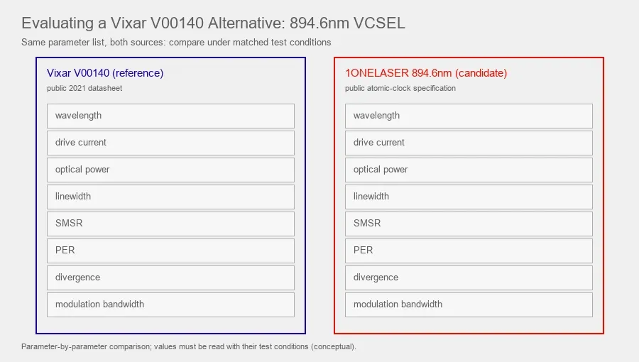
If an existing cesium atomic-clock design was developed around the Vixar V00140, the replacement question is not simply whether another VCSEL emits at 894.6nm.
The useful question is whether another source can reproduce the optical behavior that the clock actually depends on.
That requires comparing the original device and the alternative under the same operating conditions, then validating both in the same cesium vapor-cell system.
For the V00140, the public 2021 datasheet gives unusually useful information for this process. It specifies the 894.6nm wavelength groups, drive condition, threshold current, optical output, slope efficiency, SMSR, polarization extinction ratio, linewidth, FM modulation bandwidth, beam divergence, temperature coefficient, die dimensions and maximum ratings.
That gives engineers a good baseline.
1ONELASER's 894.6nm single-mode VCSEL for cesium atomic-clock development can be evaluated against that baseline. Its current public atomic-clock specification is intentionally close to the operating region used by the V00140, but it should still be treated as an evaluation candidate rather than assumed to be a drop-in replacement.
The best replacement process is therefore:
datasheet comparison → mechanical review → optical bench comparison → Cs-cell test → clock-level validation
Why the V00140 became a useful reference point
The Vixar V00140 was developed specifically for atomic-clock and magnetometer applications.
Its public datasheet identifies it as a GaAs single-mode VCSEL at 894.6nm, the cesium D1 region used in compact cesium vapor-cell systems.
The device is also offered in temperature groups.
The 2021 datasheet lists groups centered around ambient test temperatures of 60 °C, 70 °C, 80 °C, 90 °C and 100 °C, each with IF = 1.4mA and DC = 100% for nominal 894.6nm operation.
That detail matters.
It shows that the part was not designed around the idea that every die simply emits exactly 894.6nm at room temperature. The operating point is connected to the temperature group.
A replacement source should be evaluated the same way.
The question is not:
Does the label say 894.6nm
It is:
Can the source reach and hold the required Cs D1 optical condition at the current and temperature available in the clock
Why V00140 second sourcing matters now
Before the parameter detail, the practical reason this question is being asked at all.
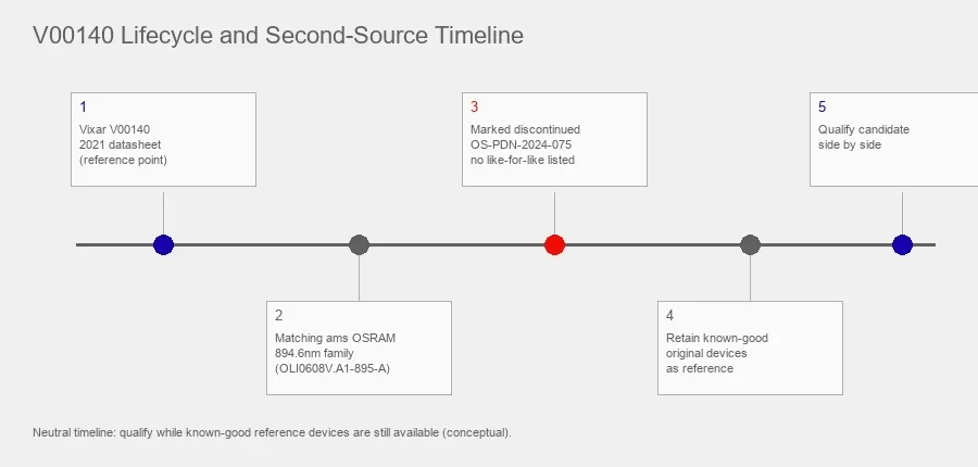
The Vixar V00140, whose 2021 datasheet is the reference used throughout this article, has a closely corresponding ams OSRAM 894.6nm / 895nm bare-die listing under OLI0608V.A1-895-A, and that current ams OSRAM product page is marked discontinued. The matching product discontinuation notice lists the five 894.6nm groups with the reason given as supply-chain instability and no drop-in replacement offered.
So the sequence for a team maintaining a V00140-based clock is:
- 1. The corresponding ams OSRAM 894.6nm family is discontinued.
- 2. The discontinuation notice does not list a like-for-like replacement.
- 3. Therefore the practical path is to qualify a second source now, side by side, while known-good original devices are still available as a reference.
The detailed lifecycle facts and the exact model-relationship wording are covered further down. The rest of this article is the parameter-by-parameter method that makes such a qualification trustworthy
The cesium transition fixes the optical target
The cesium-133 ground-state hyperfine transition defines the SI second at exactly 9,192,631,770Hz.
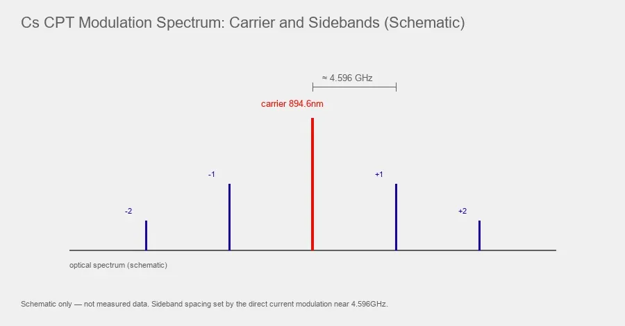
In a common CPT cesium clock architecture, the optical source is operated near the Cs D1 line around 894.6nm and can be directly current-modulated near 4.596GHz so that useful optical sidebands address the two ground-state hyperfine levels.
This is one reason modulation bandwidth matters in a replacement evaluation.
A source can match the nominal wavelength and still be unsuitable if its direct modulation response cannot generate the required optical sidebands with adequate power and stability.
Other cesium clock architectures can use different interrogation arrangements, so the 4.596GHz requirement should be tied to the actual clock design rather than treated as a universal rule for every cesium clock.
Public specification comparison
The table below compares the public Vixar V00140 data with the currently published 1ONELASER 894.6nm single-mode VCSEL data for cesium atomic-clock development.
The values should be read together with their test conditions.
Parameter | Vixar V00140 public specification | 1ONELASER 894.6nm Cs Atomic Clock VCSEL public specification | Replacement question |
|---|---|---|---|
Product form | Bare die | Bare die standard | Does the customer's assembly accept the same delivery form |
Laser architecture | GaAs single-mode VCSEL | Single-mode VCSEL bare die | Confirm mode behavior in the real operating window |
Peak wavelength | 894.6nm typ., 894.1 to 895.1nm for Group 3 test condition | 894.6nm typ., 894.1 to 895.1nm | Can both sources reach the same Cs D1 operating point |
Main reference condition | Ta = 80 °C, IF = 1.4mA, DC = 100% for Group 3 | Ta = 80 °C, IF = 1.4mA, DC = 100% | Compare at the same current and temperature |
Temperature groups | 60±10 °C through 100±10 °C groups at IF = 1.4mA | Project operating point and binning should be confirmed | Is the available wavelength bin compatible with the existing heater or TEC range |
Threshold current | 0.61mA typ. | 0.6mA typ. | Does the driver have suitable bias margin |
Operating current used for optical data | 1.4mA | 1.4mA | Can the existing driver operate at the required bias |
Maximum current while remaining single mode | 1.5mA max. at the stated Vixar condition | Not stated as a universal public maximum on the current product page | Characterize mode behavior across the customer's actual current range |
Absolute forward current | 3mA max. at stated Vixar condition | Confirm current datasheet for project device | Do not infer an absolute maximum from the nominal operating current |
Forward voltage | 1.78V typ. | 1.8V typ. | Check driver compliance and power budget |
Optical output | 0.3mW typ. at Ta = 80 °C and IF = 1.4mA | 0.3mW typ. at Ta = 80 °C and IF = 1.4mA | Compare power after the same optics and through the same vapor cell |
Ordering-description power class | 0.2mW is shown in the V00140 ordering description | Current product page publishes 0.3mW typ. at the stated test point | Do not confuse product-class wording with the characteristics-table operating point |
Slope efficiency | 0.37W/A typ. | 0.37W/A typ. in current 1ONELASER technical documentation | Compare L-I behavior around the intended bias point |
SMSR | ≥20dB | ≥20dB | Verify side-mode suppression under the actual thermal and modulation condition |
PER | ≥15dB | ≥15dB | Confirm polarization behavior after assembly |
Spectral linewidth | ≤100MHz | ≤100MHz standard specification | Decide whether the laboratory needs tighter screened devices |
FM modulation bandwidth | ≥4.6GHz | ≥4.6GHz | Test the exact clock RF frequency and optical sideband spectrum |
Beam divergence | 12° × 12° FWHM, 20° × 20° at 1/e² | 20° typ. at 1/e² | Confirm the same divergence definition before comparing |
Wavelength temperature coefficient | 0.06nm/K typ. | 0.06nm/K typ. | Check available temperature tuning range and controller resolution |
Wavelength current coefficient | Not listed in the main V00140 characteristics table reviewed here | 0.3nm/mA typ. | Characterize both sources in the customer's own setup if current tuning is used for locking |
Die footprint | 160μm × 200μm | Lateral footprint should be confirmed from the current order-specific drawing | Mechanical compatibility cannot be assumed from wavelength alone |
Die thickness | 150μm | 150μm | Check die attach height and optical axis |
V00140 operating/solder temperature maximum rating | -20 °C to 110 °C | Project-specific operating limits should be confirmed from the supplied device documentation | The package cannot override the device maximum-rating limits defined by the supplier documentation |
V00140 storage temperature | -40 °C to 125 °C | Confirm current project documentation | Qualification limits must be compared separately from operating setpoints |
ESD | V00140 explicitly lists 250V HBM Class 1A | No numeric ESD value is published on the current 1ONELASER atomic-clock product page | Use ESD-controlled assembly and request project-specific handling information rather than assuming equivalence |
This table shows why a replacement decision cannot be made from one line.
Several headline values are close.
The remaining work is to confirm whether those values remain suitable after the die is mounted, temperature-controlled, modulated and placed in the customer's optical system.
Do not compare 0.2mW and 0.3mW without reading the test condition
One small detail in the V00140 datasheet is easy to misread.
The first-page ordering description includes a 0.2mW product description.
The characteristics table for Group 3, however, gives a typical optical output of 0.3mW at Ta = 80 °C, IF = 1.4mA and DC = 100%.
Those statements are not necessarily contradictory.
One is part of the product ordering description and the other is a typical measured characteristic at a defined operating point.
When comparing an alternative source, use the characteristics under a matched test condition.
Do not take one headline number from one datasheet and compare it with a differently defined number from another.
The same rule applies to divergence, linewidth and temperature.
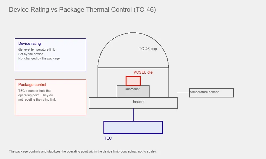
Temperature: the device rating comes first, the package only controls it
A common source of confusion in atomic-clock laser discussions is the relationship between the device temperature rating and package temperature control.
The VCSEL device has its own maximum-rating temperature limits, defined by the supplier documentation.
The V00140 datasheet, for example, specifies an operation/solder temperature range from -20 °C to 110 °C in its maximum-ratings section. This is the device maximum-rating limit stated by the supplier; it is an operation/solder rating and should not be read as a directly quoted junction-temperature limit. Its wavelength groups are then defined around selected operating temperatures inside that rated range.
A package does not widen the device's rated temperature limits.
The package performs other jobs:
- provide a thermal path
- help remove heat
- provide controlled heating or cooling
- hold a thermistor or other temperature sensor
- integrate a TEC or Peltier element
- reduce thermal gradients
- stabilize the device at the selected wavelength operating point
This distinction is important for replacement qualification. If the alternative device has a different rated temperature limit in its own documentation, putting it into the same TO package does not make it equivalent. The thermal design has to keep the device inside the safe, characterized region defined by its own datasheet.
For teams that do not want to mount and thermally control a bare die themselves, 1ONELASER supports project-specific packaged configurations for atomic-clock sources. Current options can include TO-can and TO-46 style integration, TEC or Peltier temperature control, NTC or PT1000 temperature sensing, ceramic submounts, vacuum or dry-nitrogen sealing and collimating optics depending on the project.
For an atomic-clock team, the useful advantage is repeatable thermal control around the optical setpoint. A TO-46 package with temperature sensing can make the source easier to integrate into a laboratory or OEM module. But the thermal controller should still be designed from the VCSEL wavelength-temperature relationship and the device's own rated limit from the supplier documentation.
One packaging requirement is easy to overlook if the same 894.6nm source will also feed an optically pumped magnetometer rather than only a clock. A sensitive magnetometer resolves fields at the nanotesla level or below, so the laser package near the vapor cell should avoid ferromagnetic package metals, platings and fasteners that could distort the local field or the sensor's lock point. If the replacement source is intended for a magnetometer or a shared clock-and-OPM platform, add a non-magnetic package option to the qualification checklist and confirm which package materials are used, rather than assuming a standard TO-can is field-neutral.
Threshold current and operating current should be reviewed separately
Threshold current tells you approximately where lasing begins.
It does not tell you the correct clock operating current.
For V00140 Group 3, the typical threshold current is 0.61mA, while the main optical specification is given at 1.4mA.
The datasheet also limits the forward current to 1.5mA for remaining single mode under the stated direct-current condition and temperature.
Those three current values have different meanings.
A replacement review should therefore ask:
- 1. At what current does the alternative reach threshold
- 2. At what current does it produce the required optical power
- 3. At what current does it remain single mode
- 4. At what current does it tune onto the required transition
- 5. What bias current produces the best CPT signal
- 6. How much current margin remains before mode behavior changes
The driver should then be designed around the actual useful operating region, not merely the threshold value.
Output power should be compared at the vapor cell
Both sources may publish approximately 0.3mW at a similar die operating point.
That is encouraging but not sufficient.
The atomic clock does not use datasheet output power directly.
The clock uses the optical field that reaches the vapor cell after:
- collimation
- attenuation
- polarization optics
- beam shaping
- package window loss
- alignment loss
- any beam splitter or reference cell
The most useful power comparison is therefore performed after the same optical train.
Mount the original and alternative source in equivalent conditions and record:
- source optical power
- power after the collimator
- power after polarization optics
- power entering the Cs cell
- transmitted power
- CPT resonance contrast
- CPT linewidth
- sensitivity of the clock signal to optical power
A source with slightly different raw output can still be a good alternative if the usable optical power at the cell is controllable and repeatable.
Linewidth should be treated as a project requirement rather than a brand number
The public V00140 specification gives a maximum spectral linewidth of 100MHz.
The current standard 1ONELASER 894.6nm cesium atomic-clock product also publishes ≤100MHz.
That makes the standard specifications comparable at a high level.
It does not mean every laboratory should automatically specify 100MHz.
Laser linewidth affects the way optical power overlaps the broadened atomic transition and can contribute to FM-to-AM noise and clock instability.
For some compact clocks, a conventional VCSEL linewidth is acceptable because low power, small size and direct microwave modulation are more important.
For a higher-stability experiment, the lab may want a narrower subset.
1ONELASER can review project-specific spectral screening requirements, including tighter linewidth selection where manufacturing distribution and test yield allow it.
A useful request would be:
Please evaluate 894.6nm single-mode VCSEL samples at Ta = 80 °C and IF = 1.4mA and advise whether a screened linewidth limit tighter than the standard ≤100MHz specification is available. Please state the measurement method, sample yield and whether the selected value can be maintained as a production screening criterion.
This is more useful than writing:
Need best linewidth
Tighter screening should always be connected to the laboratory's clock target.
SMSR and polarization must be checked after mounting
The V00140 publishes:
- SMSR ≥20dB
- PER ≥15dB
The current 1ONELASER standard atomic-clock source publishes the same standard values.
These parameters still need system validation.
Vixar's own datasheet notes that the polarization extinction ratio can degrade because of die stress induced by mounting or packaging.
That is a very important replacement lesson.
A bare die can pass a polarization test before assembly and behave differently after:
- die attach
- curing
- wire bonding
- package sealing
- thermal cycling
- mechanical stress
The same logic applies to side-mode behavior.
For a drop-in evaluation, repeat the spectrum and polarization measurement after the alternative is assembled in the actual package.
Compare beam divergence using the same definition
V00140 provides two divergence definitions:
- approximately 12° × 12° at FWHM
- approximately 20° × 20° at 1/e²
The 1ONELASER atomic-clock page publishes approximately 20° at 1/e².
These are consistent ways to describe different points on the same type of far-field distribution, but they are not interchangeable numbers.
Before deciding that two devices have different beam divergence, check whether both values use:
- FWHM
- 1/e²
- D86
- full angle
- half angle
This matters because beam divergence affects collimator selection and the amount of optical power collected.
If the existing V00140 package uses a fixed micro-lens, even a modest divergence change can alter the beam diameter or power at the vapor cell.
Slope efficiency tells you how power responds to current
The V00140 public characteristics table lists a typical slope efficiency of 0.37W/A.
Current 1ONELASER technical documentation for the standard Cs atomic-clock device publishes the same typical value.
Slope efficiency is useful because it links electrical bias changes to optical-power changes above threshold.
For a clock, this affects two practical questions.
First, how much power change occurs when the current is adjusted for wavelength locking.
Second, how much amplitude modulation accompanies intentional frequency modulation.
The replacement test should therefore include an L-I sweep around the actual bias current rather than comparing a single output-power point.
Temperature coefficient determines how much thermal tuning is available
V00140 publishes a wavelength temperature coefficient of approximately 0.06nm/K.
The current 1ONELASER atomic-clock product publishes the same typical value.
This gives a first estimate of how much the laser wavelength moves when the controlled die temperature changes.
For example, a few kelvin of temperature shift can move the center wavelength by several tenths of a nanometer.
That is useful for bringing the laser onto the Cs D1 line.
It also means poor thermal stability becomes frequency drift.
A replacement source should therefore be tested with the actual heater or TEC controller.
Record:
- temperature setpoint
- measured package or die-adjacent sensor temperature
- peak wavelength
- optical power
- warm-up time
- wavelength drift after thermal equilibrium
- clock error signal after stabilization
Do not compare only the coefficient printed on the datasheet.
Compare how the complete source is controlled.
FM modulation bandwidth is critical for a CPT clock
The V00140 specifies a minimum FM modulation bandwidth of 4.6GHz.
The current 1ONELASER atomic-clock source specifies ≥4.6GHz.
That is directly relevant to compact Cs CPT architectures that operate around 4.596GHz.
However, a bandwidth number alone does not prove identical clock behavior.
The engineer should compare the modulated optical spectrum.
Measure:
- carrier power
- first-order sideband power
- sideband symmetry
- modulation index
- RF drive power
- bias current
- residual amplitude modulation
- spectrum versus temperature
The practical acceptance question is:
Can the alternative generate the optical spectrum that gives the required CPT resonance in the existing clock
That is more meaningful than whether both datasheets print 4.6GHz.
Mechanical compatibility deserves its own review
The V00140 drawing shows a die approximately:
- 160μm wide
- 200μm long
- 150μm thick
It also shows the anode bonding area, emitting aperture location and polarization direction.
The current 1ONELASER product page publicly states a 150μm die thickness but does not expose all lateral footprint and pad dimensions in the indexed product text.
For a replacement project, request the current mechanical drawing before assuming physical compatibility.
Check:
- die length
- die width
- thickness
- cathode arrangement
- anode bond-pad position
- emitting aperture position
- polarization-axis reference
- die-edge clearance
- wire-bond loop geometry
A source can be optically suitable and still fail the replacement project because the existing submount or wire-bond fixture cannot accept the new pad geometry.
ESD should be handled carefully in a bare-die comparison
It is common for engineers to think of ESD mainly as an assembly and package-handling issue.
That is reasonable, but it should not be turned into a rule that bare-die datasheets never contain ESD values.
The V00140 is a clear counterexample.
Its 2021 bare-die datasheet explicitly lists an ESD withstand voltage of 250V according to ANSI/ESDA/JEDEC JS-001 HBM Class 1A.
The current public 1ONELASER atomic-clock product page does not publish a numeric ESD withstand rating.
Therefore an alternative-source table should not write “same ESD” unless the value has actually been provided for the project device.
The correct engineering action is:
- handle bare die in an ESD-controlled process
- request the relevant supplier handling specification
- review package-level protection separately
- define the customer's own assembly ESD controls
- do not infer a missing ESD rating
This is a good example of why a replacement table should include “not publicly stated” when a value is not available.
How to describe the Vixar and ams OSRAM model relationship accurately
Current search results can create confusion around Vixar and ams OSRAM part numbers.
The current ams OSRAM page for OLI0608V.A1-895-A describes an 895nm VCSEL bare die with 1.4mA current, 0.3mW optical output, 20° beam angle, 0.20mm × 0.16mm × 0.15mm dimensions and -20 °C to 110 °C operating temperature.
The current OLI0608V.A1-895-A datasheet goes further and lists the device as a GaAs VCSEL at 894.6nm, single-mode radiation profile, 250V ESD to ANSI/ESDA/JEDEC JS-001 HBM Class 1A, and exactly the same five temperature groups the Vixar part used: Group 1 to Group 5 at Ta = 60/70/80/90/100 °C, each specified at IF = 1.4mA and DC = 100% for 894.6nm, with ams OSRAM ordering codes (for example Q65113A6387 for Group 1 and Q65113A7969 for Group 3).
That combination of 894.6nm, single-mode operation, identical ESD class, identical temperature-group structure and matching drive condition is strong evidence that the current ams OSRAM 895nm bare die is the continuation of the former Vixar V00140 device family.
The same ams OSRAM page also includes downloadable images labeled “V00145, V00140,” which reinforces that catalog relationship.
However, unless a formal official part-number mapping document explicitly states that one specific Vixar ordering code is identical to one specific OSRAM ordering code, the safest wording is:
corresponding ams OSRAM 895nm model
or:
related current ams OSRAM listing for the former Vixar product family
Do not write:
V00140 is exactly OLI0608V.A1-895-A
unless the formal mapping document is available.
This distinction is small but important for a technical replacement article.
The corresponding ams OSRAM 894.6nm family is now on an official discontinuation notice
The lifecycle summary at the top of this article can be stated more precisely here.
The current ams OSRAM product page for OLI0608V.A1-895-A is marked discontinued, and the product discontinuation notice lists all five 894.6nm groups, gives the reason as supply-chain instability, and offers no drop-in replacement.
One detail is worth adding: the discontinuation is not limited to the cesium part. The corresponding 795nm rubidium bare die from the same BIDOS family is on the same notice, so teams running rubidium D1 systems on the former 795nm die face the same second-source question.
Because there is no like-for-like replacement listed, a customer's own qualification becomes the continuity path, and the useful qualification data can only be gathered while known-good original devices are still on hand as a reference.
Note that obsolescence status, notice numbers and any last-time-buy or last-time-ship dates can change after publication. Confirm the current status directly with ams OSRAM or an authorized distributor before making a lifecycle decision.
More than one second source may exist, so qualify by function
Since the original Vixar part reached end of life, potential second-source candidates are available in the 894.6nm and 895nm single-mode VCSEL market, offered as bare die and as packaged devices with integrated temperature control. Each candidate still requires device-specific qualification.
That availability is good for supply resilience, but it changes the engineering question only slightly.
The task is not to find the source whose datasheet looks closest to the V00140 on paper. It is to qualify a specific candidate device, from a specific supplier, at a specific operating point, in your own cesium cell.
The comparison method in this article is deliberately source-neutral for that reason. The same datasheet-to-cell workflow applies whether the candidate is the 1ONELASER 894.6nm VCSEL or any other 894.6nm source, and the qualification data only becomes meaningful once it is measured against your retained known-good reference part.
What 1ONELASER can screen for a project
The standard public specification should be treated as the starting point.
For a laboratory with tighter requirements, 1ONELASER can review project-specific screening or binning requests such as:
- narrower wavelength bin
- defined operating-temperature group
- tighter linewidth selection
- higher SMSR subset
- higher PER subset
- optical-power range
- wavelength tuning behavior
- current operating window
- package configuration
Not every combination will be available at production yield.
A request for a tighter limit should therefore include:
- exact test temperature
- exact current
- CW or modulated operation
- measurement method
- quantity
- acceptable yield or cost tradeoff
- whether the value is for sample selection or production guarantee
That gives the supplier enough information to determine whether the requested bin can be supported.
A practical side-by-side qualification plan
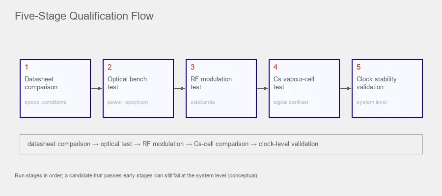
A replacement program can be organized in five stages.
Stage 1
Electrical and mechanical incoming inspection.
Measure:
- die dimensions
- bond-pad geometry
- forward voltage
- threshold current
- L-I curve
- ESD handling process
Stage 2
Free-running optical characterization.
At the same current and temperature for both devices, measure:
- peak wavelength
- output power
- linewidth
- SMSR
- PER
- beam divergence
- wavelength versus temperature
- wavelength versus current
Stage 3
RF modulation characterization.
At the intended Cs clock modulation frequency, compare:
- S11 or electrical response if relevant
- optical modulation response
- carrier and sideband power
- modulation index
- sideband symmetry
- residual amplitude modulation
Stage 4
Cs vapor-cell comparison.
Using the same cell and optical path, record:
- absorption spectrum
- wavelength lock point
- transmitted optical power
- CPT contrast
- CPT linewidth
- error-signal slope
Stage 5
Clock-level validation.
Measure:
- warm-up behavior
- short-term frequency stability
- long-term drift
- light-shift sensitivity
- temperature sensitivity
- current sensitivity
- unit-to-unit variation
Only after these stages should the new source be called qualified for that specific clock.
A replacement qualification table you can send to a supplier
Requirement | Customer should provide |
|---|---|
Reference source | Vixar V00140 group and original datasheet revision |
Atomic species | Cs-133 |
Optical line | D1 around 894.6nm |
Clock architecture | CPT or other |
Nominal laser temperature | Exact setpoint |
Temperature range | Minimum and maximum |
Bias current | Nominal and range |
Optical power | Required at source or cell |
Linewidth | Standard acceptable or tighter target |
SMSR | Minimum required |
PER | Minimum required |
RF modulation | Exact frequency and required response |
Beam divergence | Definition and maximum |
Die mechanics | Footprint, thickness and bond-pad constraints |
Package | Bare die, TO-46, TEC, NTC/PT1000 or other |
ESD | Assembly control and required rating if applicable |
Validation quantity | Sample count |
Production quantity | Forecast volume |
This creates a useful technical conversation instead of asking a supplier for “a V00140 equivalent.”
Final engineering rule
An alternative to the Vixar V00140 should be qualified by function, not by product name.
The public V00140 specification gives a strong reference set:
- 894.6nm nominal wavelength
- 1.4mA reference operating current
- 0.61mA typical threshold current
- 0.3mW typical output at the Group 3 test point
- 0.37W/A typical slope efficiency
- ≥20dB SMSR
- ≥15dB PER
- ≤100MHz linewidth
- ≥4.6GHz FM modulation bandwidth
- approximately 20° divergence at 1/e²
- 0.06nm/K wavelength temperature coefficient
- 160μm × 200μm × 150μm die geometry
The current 1ONELASER 894.6nm Cs atomic-clock VCSEL publishes closely aligned values for many of these optical parameters and supports project-specific screening and optional temperature-controlled package configurations.
That makes it a reasonable evaluation candidate.
It does not make it an automatic drop-in replacement.
The final replacement decision should come from the cesium vapor cell and the clock output.
For current product data, review the 894.6nm Single Mode VCSEL for Cs Atomic Clock product page. For the broader source platform, review the Atomic Clock and OPM Magnetometer Solution.
Frequently Asked Questions
Is the 1ONELASER 894.6nm VCSEL a drop-in replacement for Vixar V00140
It should be treated as an engineering evaluation candidate, not a guaranteed drop-in replacement. Several public optical specifications are closely aligned, but mechanical, thermal, modulation and vapor-cell performance should be validated in the customer's actual clock.
What is the Vixar V00140 linewidth
The 2021 public V00140 datasheet specifies a maximum spectral linewidth of 100MHz at its defined Group 3 operating condition. A laboratory that needs a tighter linewidth should define the required operating point and measurement method rather than assuming the standard value is optimal.
Can 1ONELASER screen parts for a tighter linewidth
Project-specific spectral screening can be reviewed according to the requested linewidth, operating current, temperature, quantity, test method and achievable production yield. A tighter value should be confirmed for the actual project rather than assumed from the standard datasheet.
Does a TO-46 package determine the VCSEL operating temperature
No. The semiconductor device has its own maximum-rating limit defined by the supplier documentation. A TO-46 package, TEC and temperature sensor help remove heat and stabilize the device at the desired operating point. They do not widen the device's rated temperature range.
Does the V00140 bare-die datasheet include an ESD rating
Yes. The reviewed 2021 V00140 bare-die datasheet explicitly specifies 250V HBM Class 1A. If an alternative bare-die product does not publish an ESD value, do not assume it is identical.
Is V00140 the same part number as OSRAM OLI0608V.A1-895-A
The current ams OSRAM OLI0608V.A1-895-A page shows closely corresponding 895nm bare-die parameters and includes product images labeled V00145 and V00140. Until a formal part-number mapping document is available, it is safer to describe it as a corresponding or related ams OSRAM model rather than state that the part numbers are exactly identical.
Is the ams OSRAM OLI0608V.A1-895-A still available
At the time of writing it is marked discontinued and appears on ams OSRAM product discontinuation notice OS-PDN-2024-075, which lists the five 894.6nm cesium groups with no direct replacement and cites supply-chain instability. The corresponding 795nm rubidium groups are on the same notice. Because obsolescence dates and last-time-buy windows change, confirm the current status with ams OSRAM or an authorized distributor, and treat a qualified second source as the practical continuity path rather than waiting for a like-for-like replacement..