Product Overview
1. Standard Bare Die VCSEL for 850nm NIR Sensing and Illumination
This 850nm 100mW VCSEL bare die is designed for near-infrared sensing, machine vision auxiliary illumination, consumer electronics optical sensing, industrial detection, and compact optical source module development.
The product is supplied as a standard bare die device by default. It is suitable for NIR sensing modules, proximity sensing evaluation, machine vision light source development, industrial optical detection systems, and chip-level VCSEL integration projects.
With 100mW-class optical output power and 120mW typical output at IF = 140mA, this device provides a stronger 850nm VCSEL source than low-power sensing chips, while still supporting compact bare die integration and customized package development.
2. Key Features
This 850nm 100mW VCSEL bare die is supplied as a standard multi-emitter VCSEL chip for medium-power NIR sensing and compact illumination applications.
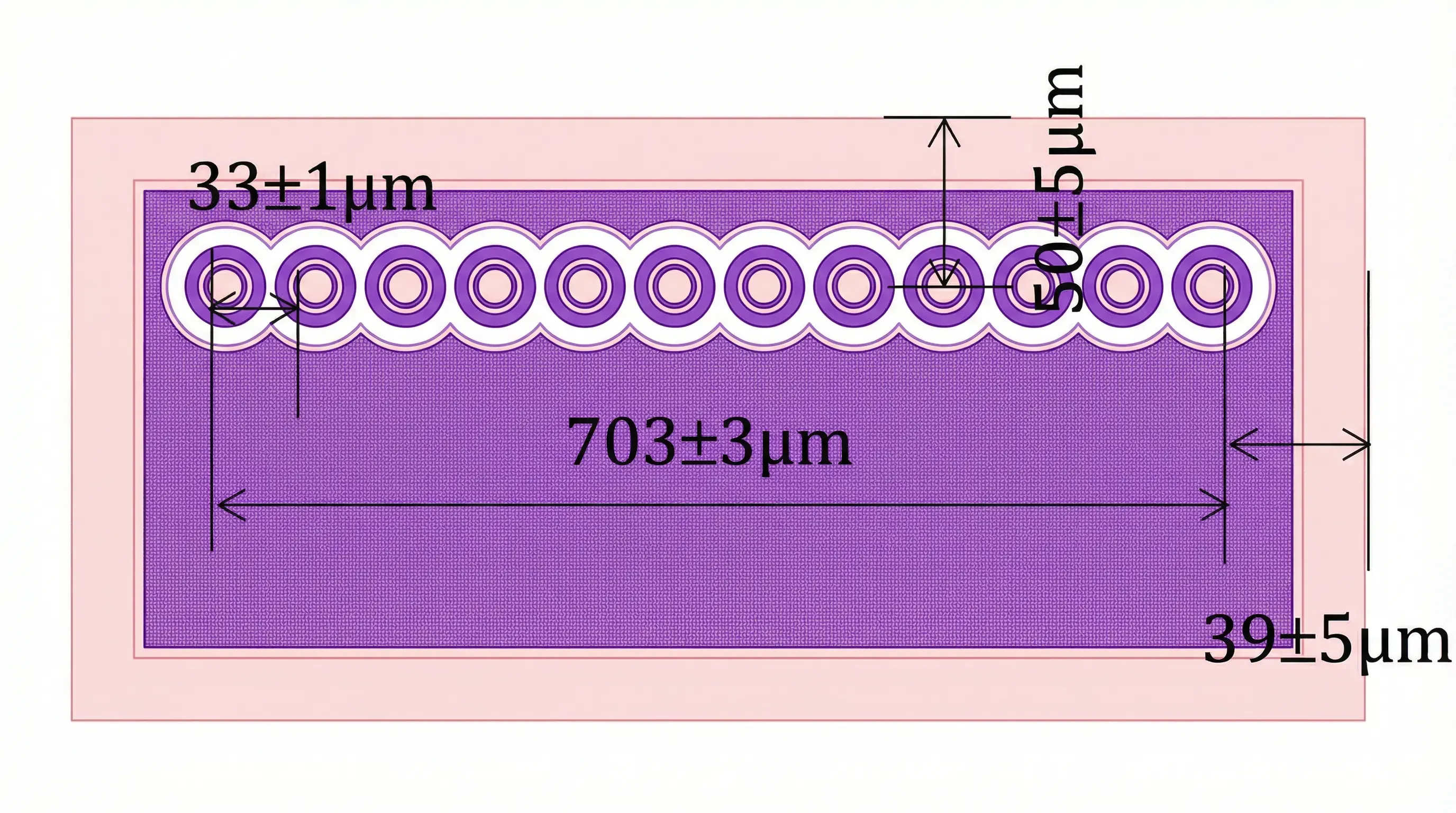
Key features include 850nm typical wavelength, 100mW-class optical output power, 120mW typical output at IF = 140mA, 22-emitter bare die structure, 10±1μm emitting aperture, 20° typical beam divergence at 1/e², stable central wavelength, and doughnut-shaped symmetrical far-field output.
The bare die format allows flexible integration into ceramic submounts, chip-on-board assemblies, compact optical modules, and customer-specific VCSEL packages.
Package-level assembly, wire bonding, ceramic submount mounting, beam shaping, divergence control, and customer-specific optical spot requirements can also be reviewed according to the customer's optical and mechanical layout.
3. Application Development Direction
This device supports 850nm NIR sensing, machine vision auxiliary illumination, consumer electronics optical sensing, proximity sensing, industrial detection, and compact VCSEL optical source integration.
In a sensing or illumination module design, the VCSEL wavelength, output power, drive current, beam profile, detector response, optical path, package structure, thermal condition, and final system signal behavior should be reviewed together.
The 100mW-class output power provides a useful medium-power source option for compact optical path design, especially where higher optical power than low-power sensing VCSELs is required while maintaining bare die assembly flexibility.
4. Evaluation Sample Kit and Documentation Support
Evaluation Sample Kit: USD 29 / KIT, 10 PCs / KIT. International express shipping is typically USD 69–89 depending on destination.
BestLaser Opto Component Device Limited has filed an Initial Product Report with the U.S. FDA CDRH for the Laser Diode Series, including the VCSEL Laser Diode Chip Series. CE-related documentation is also available for project evaluation, including EMC documentation and EN 60825 laser safety / LVD test documentation. Material compliance documentation, including RoHS, REACH, and HF documentation, can also be provided upon request.
For 850nm sensing, machine vision, and compact optical source projects, bare die mounting, ceramic submount assembly, chip-on-board integration, wire bonding, beam shaping, or customized package discussion is available according to the project requirements.
Please contact us for sample testing, engineering evaluation, or custom project support.
850nm 100mW VCSEL Bare Die Datasheet Download ↓