
940nm
940nm VCSEL Bare Die Series
940nm VCSEL bare die series from 5mW to 8W for NIR sensing, pulsed illumination, machine vision, industrial detection and custom optical modules.
Specifications
- Product Type
- VCSEL Bare Die Series
- Wavelength
- 940nm typ.
- Optical Output Power
- 5mW / 20mW / 30mW / 100mW / 300mW / 500mW / 800mW / 1W / 1.5W / 2W / 3W / 6W / 8W
- Emitter Configuration
- 1 emitter to 1273 emitters, depending on product version
- Operating Mode
- QCW / Pulse operation
- Die Size
- 163μm × 170μm to 1340μm × 1500μm, depending on product version
- Recommended Assembly
- Wire bonding / ceramic submount / custom packaging
1. 940nm VCSEL Bare Die Supply for Packaging and Module Integration
The 940nm 5mW–8W VCSEL Bare Die Series includes low-power single-emitter devices, compact multi-emitter chips, medium-power NIR sources and high-power VCSEL arrays for semiconductor packaging and custom optical-module integration.
The available optical-output classes include 5mW, 20mW, 30mW, two 100mW die formats, 300mW, 500mW, 800mW, 1W, 1.5W, 2W, 3W, 6W and 8W models. These products support QCW or Pulse operation according to the selected configuration and corresponding product datasheet.
The series provides a typical center wavelength of 940nm within a specified 930nm – 950nm wavelength range. Depending on the model, the devices contain from one emitter to 1,273 emitters and provide typical beam-divergence values from 19° to 29° at 1/e².
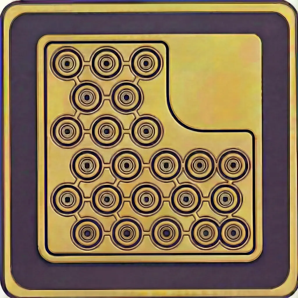
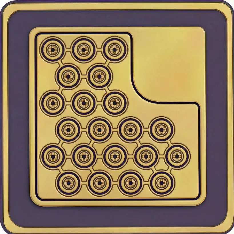
These 940nm multi-mode VCSEL devices are supplied as unpackaged semiconductor bare dies for conductive die attachment, gold-wire bonding, ceramic-submount assembly, chip-on-board integration, custom VCSEL packaging and application-specific optical-source development.
The different output levels, emitter configurations, die dimensions, forward-voltage requirements and beam-divergence values allow customers to select a suitable chip according to package space, target optical output, pulse condition, driver capability, thermal path, optical field and system architecture.
This series is intended for:
- OSAT semiconductor assembly and test providers
- VCSEL and laser-diode packaging companies
- SMD, TO-can and ceramic laser-package manufacturers
- Die-attach and gold wire-bonding engineering teams
- Ceramic-submount and COB integrators
- NIR sensing and active-illumination developers
- Machine-vision and industrial-detection companies
- Lens, diffuser, collimation and beam-shaping companies
- Consumer-electronics optical-source developers
- Laser-component and optical-module distributors
- Technical sourcing and second-source development teams
As a 940nm VCSEL bare die supplier, 1ONELASER supports model selection, evaluation samples, power-bin discussion, ceramic-submount integration, custom packaging and optical-module development.
The devices can be integrated into custom SMD packages, TO-can packages, ceramic laser packages, ceramic-submount assemblies, COB optical sources and application-specific near-infrared modules. These products require appropriate die mounting, wire bonding, package protection, thermal-path design and optical integration before use in a finished device.
Lead Time: In-stock products are dispatched within 3 business days; custom-packaged products have a lead time of 15–20 days.
MOQ: The minimum order quantity is 1 reel; selected special models support small-batch orders.
2. 5mW to 8W VCSEL Bare Die Model Selection
The 940nm VCSEL Bare Die Series covers low-power sensing devices, medium-power illumination chips and high-power multi-emitter arrays.
All models in the following table support QCW or Pulse operation. Model selection should consider optical output, test current, forward voltage, emitter count, die dimensions, beam divergence, pulse width, duty cycle, package structure, thermal path and final optical-system requirements.
Product | Optical Output | Current / Voltage | Emitters | Die Size | Beam Divergence |
|---|---|---|---|---|---|
940nm 5mW | 5mW min. 6mW typ. | 7mA 1.9V typ. | 1 | 170 × 170μm | 21° typ. 1/e² |
940nm 20mW | 20mW min. 24mW typ. | 28mA 1.95V typ. | 4 | 170 × 170μm | 21° typ. 1/e² |
940nm 30mW | 30mW min. 36mW typ. | 42mA 1.95V typ. | 6 | 163 × 185μm | 21° typ. 1/e² |
940nm 100mW 10Mil | 100mW min. 115mW typ. | 140mA 2.0V typ. | 23 | 245 × 239μm | 21° typ. 1/e² |
940nm 100mW 13Mil | 100mW min. 120mW typ. | 140mA 2.0V typ. | 21 | 300 × 300μm | 21° typ. 1/e² |
940nm 300mW | 275mW min. 290mW typ. 320mW max. | 350mA 2.0V typ. | 48 | 330 × 330μm | 20° typ. 1/e² |
940nm 500mW | 500mW min. 580mW typ. | 700mA 2.0V typ. | 95 | 575 × 555μm | 21° typ. 1/e² |
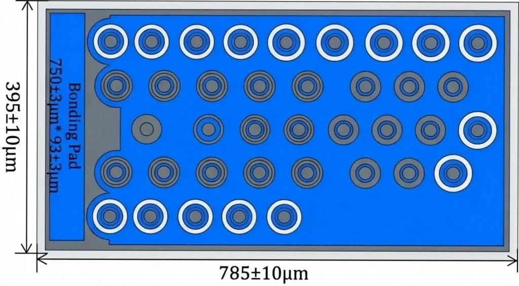
940nm 800mW | 780mW min. 830mW typ. | 0.5A 3.4V typ. | 44 | 785 × 395μm | 29° typ. 1/e² |
940nm 1W | 1W min. 1.15W typ. | 1.4A 2.1V typ. | 201 | 775 × 670μm | 21° typ. 1/e² |
940nm 1.5W | 1.5W min. 1.65W typ. | 2A 2.1V typ. | 280 | 885 × 810μm | 21° typ. 1/e² |
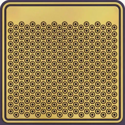
940nm 2W | 2W min. 2.2W typ. | 2.8A 2.1V typ. | 410 | 995 × 1020μm | 21° typ. 1/e² |
940nm 3W | 3W min. 3.3W typ. | 4A 2.1V typ. | 624 | 1075 × 1120μm | 21° typ. 1/e² |
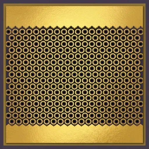
940nm 6W | 5W min. 5.5W typ. 6W max. | 7A 2.2V typ. | 1,273 | 1340 × 1500μm | 19° typ. 1/e² |
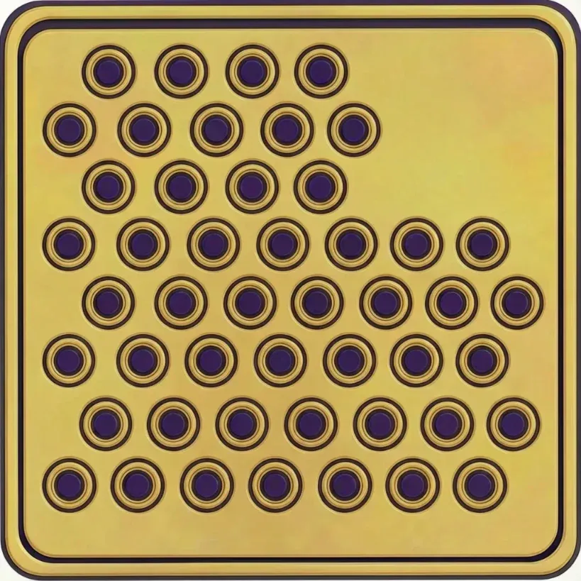
940nm 8W | 8W min. 9W typ. 10W max. | 3.5A 4.9V typ. | 560 | 910 × 770μm | 28° typ. 1/e² |
The optical-output values, test currents and electrical characteristics are model-specific. Exact pulse width, duty cycle, temperature and test conditions should be confirmed in the corresponding product datasheet.
A wattage value measured under one pulse condition should not be interpreted as directly equivalent to continuous-wave output or to another device tested under different pulse conditions.
940nm 5mW, 20mW and 30mW VCSEL Bare Die
The 5mW, 20mW and 30mW devices are compact low-power options for initial die-attach trials, wire-bonding validation, NIR sensing, proximity-source development, short-distance optical detection and compact optical modules.
The 5mW model uses one emitter, while the 20mW and 30mW chips use four and six emitters respectively. Their compact die dimensions allow evaluation in space-constrained package designs.
940nm 100mW 10Mil and 13Mil VCSEL Bare Die
Two 100mW VCSEL bare die formats are available. The 10Mil version uses 23 emitters in a 245 × 239μm die and provides 115mW typical optical output. The 13Mil version uses 21 emitters in a 300 × 300μm die and provides 120mW typical output.
The two configurations are not mechanically identical. Selection should consider package space, die dimensions, emitter layout, die-attach area, bond-pad position and the customer's optical-source architecture.
940nm 300mW, 500mW, 800mW and 1W VCSEL Bare Die
The 300mW, 500mW, 800mW and 1W models provide medium-power options for active NIR illumination, machine-vision support, industrial sensing, consumer-electronics source development and compact optical modules.
The 800mW chip differs electrically and optically from the other models in this group. It provides 830mW typical output at 0.5A, has a 3.4V typical forward voltage and a 29° typical beam-divergence value. These parameters should be considered during driver and optical design.
940nm 1.5W, 2W and 3W VCSEL Bare Die
The 1.5W, 2W and 3W devices are high-power multi-emitter arrays developed for stronger pulsed NIR illumination, industrial optical detection, machine-vision source development and custom VCSEL module integration.
These arrays require package designs that support higher pulse current, effective die attachment, current distribution, wire-bond capacity and a controlled thermal path.
940nm 6W and 8W VCSEL Bare Die
The 6W and 8W devices are the highest-power selected configurations in the current 940nm series. The 6W model uses 1,273 emitters and provides 5.5W typical output at 7A. The 8W model uses 560 emitters and provides 9W typical output at 3.5A.
The devices use different die structures, electrical characteristics and beam-divergence values. They should not be treated as interchangeable versions of the same design. Driver capability, package parasitics, wire-bond structure, thermal path and external optics should be evaluated separately.
3. Packaging, Optical Module and Application Development
OSAT and Custom VCSEL Packaging
The 940nm VCSEL bare dies can be supplied for conductive die attachment, gold-wire bonding, ceramic-submount assembly, custom SMD packages, TO-can packages, ceramic laser packages and chip-on-board optical-source integration.
Packaging and integration directions include:
- VCSEL die attachment
- Gold-wire bonding
- Ceramic-submount assembly
- Custom VCSEL packaging
- Custom SMD laser packages
- TO-can laser packages
- Ceramic laser packages
- COB optical-source assemblies
- Multi-emitter VCSEL array modules
- Application-specific NIR source packages
The package should be designed according to the selected die dimensions, bond-pad configuration, test current, forward voltage, emitter layout, optical output and thermal requirements.
The dies are ESD-sensitive semiconductor components. Appropriate electrostatic-control procedures are required throughout storage, handling, die placement, wire bonding, package assembly and testing.
Lens, Diffuser and Beam-Shaping Integration
The series can support optical companies developing lens-integrated, diffuser-integrated, collimated or beam-shaped 940nm near-infrared source assemblies.
Possible integration directions include:
- Collimation-lens assemblies
- Beam-shaping optical components
- Diffuser-integrated VCSEL modules
- Lens-integrated NIR sources
- FOV-controlled illumination modules
- Machine-vision illumination sources
- Application-specific optical assemblies
The devices provide a symmetrical doughnut-shaped far-field profile. Final optical performance depends on the selected VCSEL chip, emitter arrangement, beam divergence, lens or diffuser design, working distance, package structure and mechanical alignment.
NIR Sensing, Machine Vision and Optical Module Development
The 940nm VCSEL Bare Die Series supports development and evaluation in the following directions:
- Near-infrared sensing
- Proximity and presence detection
- Short-distance optical detection
- Active NIR illumination
- Machine-vision support lighting
- Industrial optical detection
- Industrial inspection systems
- Custom optoelectronic modules
- Engineering and research light sources
For application-level source selection and optical-system planning, visit the Sensing & Machine Vision solution page.
Consumer Electronics and Active Illumination Development
The low-power and medium-power chips can support development of compact 940nm optical sources for consumer electronics, proximity sensing, presence detection, active illumination and embedded NIR modules.
The higher-power arrays can support projects requiring greater pulsed optical output, larger emitter configurations and custom package or module integration.
Final source performance depends on the VCSEL die, pulse driver, package, thermal path, optical components, detector response, signal-processing architecture and operating environment.
For broader packaging, thermal and optical-module development, visit the High-Power NIR & Optical Modules solution page.
Distribution and Supply-Chain Support
The 940nm VCSEL Bare Die Series is available to laser-component distributors, optical-module suppliers, technical sourcing companies and second-source development teams supporting customer packaging and integration projects.
We provide documentation, evaluation samples, model selection, power-bin requirements and volume-supply planning according to the project stage.
Related Articles
4. Evaluation Kit and Documentation Support
The 940nm VCSEL Bare Die Series is available as an Evaluation Kit for die-attach trials, wire-bonding development, package evaluation, driver testing and initial optical integration.
The Evaluation Kit includes 10 pcs / KIT per selected model:
Samples & Pilot Production: Evaluation kits, low-volume pilot production, and pre-production validation are supported.
- One selected 940nm VCSEL bare die model per kit
- Corresponding product datasheet
- Die-dimension and assembly documentation
- International shipping quoted according to destination
We offer project-specific support for the following requirements:
- Center wavelength
- Wavelength tolerance
- Optical output power
- Power-bin selection
- QCW or Pulse operating requirements
- Emitter configuration
- Die size and bond-pad layout
- Ceramic-submount requirements
- Custom SMD, TO-can or ceramic packaging
- Lens, diffuser and beam-shaping integration
- Optical-module development
- Volume-supply requirements
For component-level project evaluation, an Initial Product Report covering the Laser Diode Series and VCSEL Laser Diode Chip Series has been filed with the U.S. FDA CDRH. This filing supports technical documentation and product evaluation.
For applicable products, CE, EMC, EN 60825, LVD, RoHS, REACH and halogen-free certification and compliance documents are available. Documentation depends on the corresponding product model and does not represent certification of the customer's finished device.
5. Frequently Asked Questions
FAQ 1. What power options are included in the 940nm VCSEL Bare Die Series?
The series includes 5mW, 20mW, 30mW, two 100mW configurations, 300mW, 500mW, 800mW, 1W, 1.5W, 2W, 3W, 6W and 8W models. The range covers compact single-emitter chips, low-power multi-emitter dies and high-power VCSEL arrays.
Each model has different test current, forward voltage, emitter count, die dimensions and beam divergence. Selection should therefore be based on the complete electrical, mechanical and optical requirements rather than nominal optical-output power alone.
FAQ 2. How should I select a 940nm VCSEL bare die for sensing or active illumination?
Selection should consider required optical output, pulse width, duty cycle, test current, forward voltage, emitter configuration, die dimensions, package space, working distance, detector response and required illumination field.
Low-power models support compact sensing and proximity-source development. Medium-power chips support active illumination and machine-vision evaluation, while higher-power arrays support stronger pulsed illumination and custom optical modules. Final selection should be confirmed using the corresponding datasheet and the customer's actual driver, package and optical architecture.
FAQ 3. What packaging and integration steps are required for a 940nm VCSEL bare die?
The products are supplied as unpackaged semiconductor dies and require die attachment, wire bonding, package protection, ESD control and an appropriate electrical and thermal path. Higher-power arrays also require careful consideration of pulse-current distribution, bond-wire capacity and package parasitics.
External lenses, diffusers or collimators may be added according to the required optical field. Final performance must be validated after packaging because the driver, package structure, thermal conditions, optical alignment and external components all affect the completed source.