
665nm+940nm
665nm 10mW / 940nm 9mW Dual-Wavelength VCSEL SMD 7015
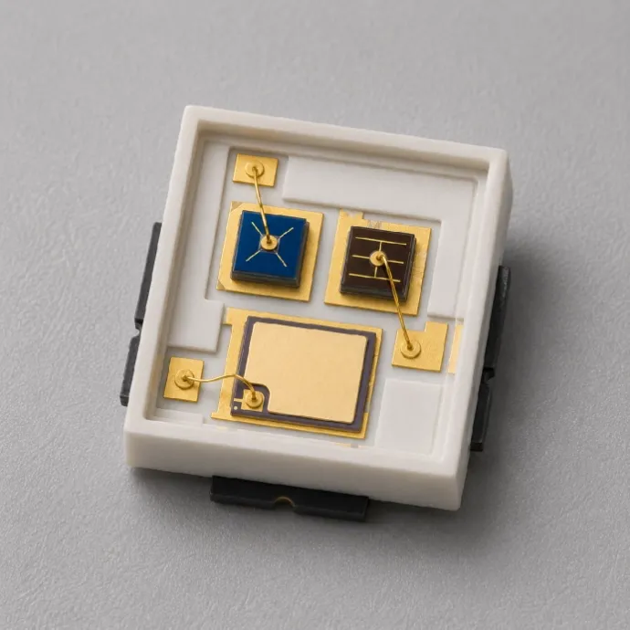
665nm 10mW and 940nm 9mW dual-wavelength VCSEL SMD in a compact 7015 package for reflective optical-system and PPG component-level OEM evaluation.
Specifications
- Product Type
- Dual-Wavelength VCSEL SMD
- Wavelength Channels
- 665nm and 940nm
- Optical Output Power
- 665nm: 10mW typ. at 15mA (9–11mW); 940nm: 9mW typ. at 15mA (8–10mW)
- Emitter Configuration
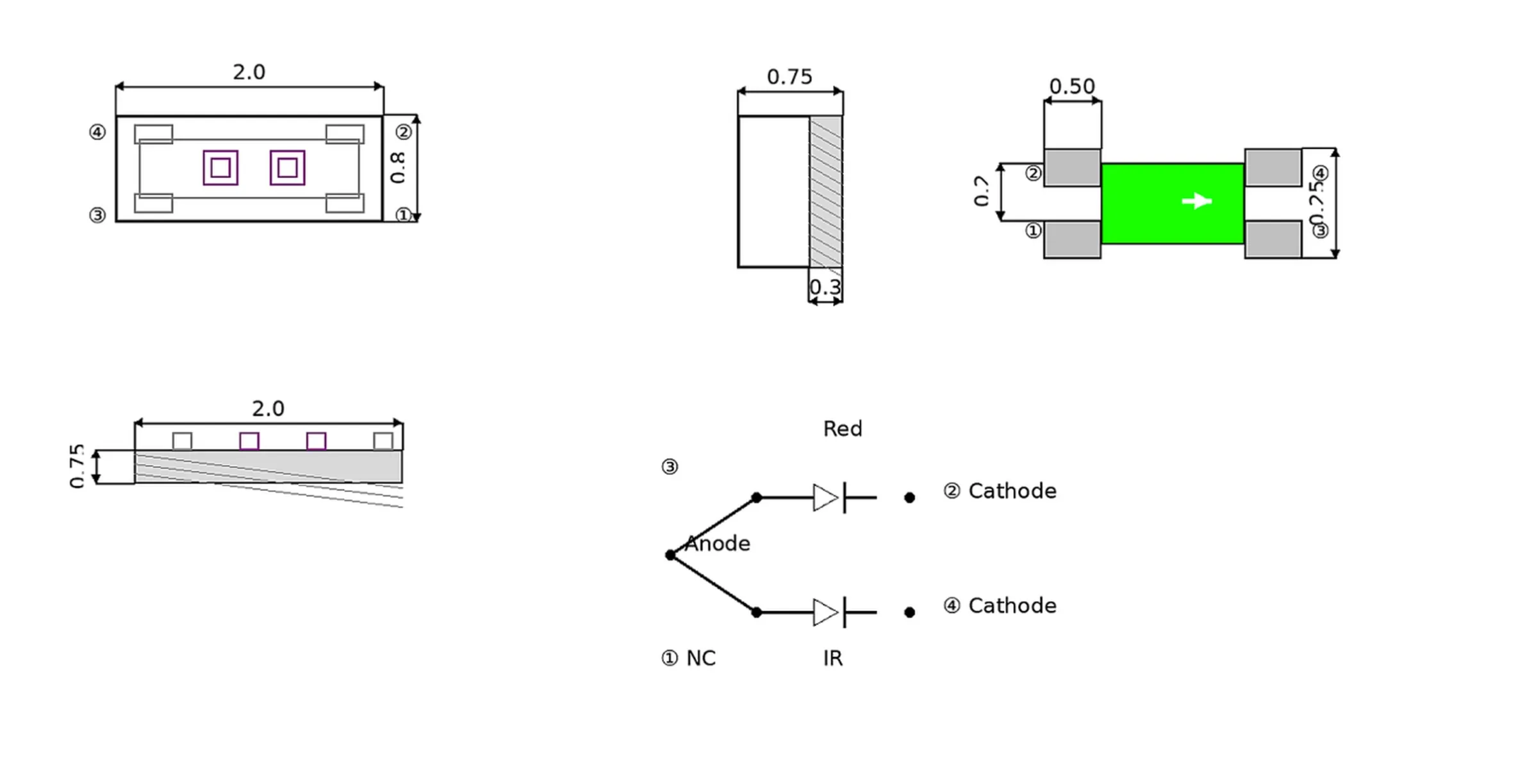
- Common-anode dual-channel layout with separate red and infrared cathodes
- Operating Mode
- CW test conditions
- Optical Emission Profile
- 20° typical FWHM beam divergence
- SMD Package Options
- 7015 SMD package, 2.0 × 0.8 × 0.75mm
1. 665nm / 940nm Dual-Wavelength VCSEL SMD for Reflective PPG Optical-System Evaluation
The 665nm 10mW / 940nm 9mW Dual-Wavelength VCSEL SMD 7015 combines a visible red 665nm channel and a 940nm infrared channel in a compact surface-mount package. It is intended for component-level evaluation of reflective optical systems and PPG-oriented OEM assemblies where a higher source-output configuration must be assessed with the customer's driver, optical geometry, detector path, and signal-processing chain.
The source specifies a 2.0 × 0.8 × 0.75mm 7015 package, water-clear encapsulation, CW test conditions, and a 20° typical FWHM beam divergence for both channels. The 665nm channel is 10mW typical at 15mA, and the 940nm channel is 9mW typical at 15mA. These are component test conditions, not a finished-device signal-quality, SpO2, accuracy, or clinical-performance specification.
Lead Time: In-stock products are dispatched within 3 business days; custom-packaged products have a lead time of 15–20 days.
MOQ: The minimum order quantity is 1 reel; selected special models support small-batch orders.
2. Multi-Wavelength Optical Configuration and Channel Selection
The package combines one red and one infrared VCSEL channel for reflective optical-system evaluation. The 665nm channel is specified at 9–11mW with 10mW typical output at 15mA. The 940nm channel is specified at 8–10mW with 9mW typical output at 15mA. Both channels use the source-stated 15mA test-current condition for this higher-output configuration.
Selection for a PPG-oriented assembly should consider the customer's optical geometry, detector response, channel timing, drive current, beam distribution, mechanical placement, optical coupling, ambient-light control, thermal behavior, and algorithm validation plan. Higher component output does not by itself establish better signal quality, SpO2 accuracy, algorithm performance, medical efficacy, or finished-device compliance.
3. 7015 Package, Electrical Interface and PCB Integration
The 7015 package uses a common-anode layout with separate red and infrared cathodes. The water-clear encapsulation and source-specified 20° typical FWHM divergence should be considered when evaluating optical-axis placement, beam overlap, diffuser or lens coupling, detector geometry, and thermal conditions at the higher-output drive point.
Before PCB release, verify the common-anode connection, separate channel current control, pad layout, reflow profile, package orientation, thermal path, optical measurement method, and mechanical clearance. Similar package dimensions or channel names do not by themselves prove pin compatibility or drop-in replacement status for another emitter.
4. Reflective PPG Optical-System Evaluation and Custom Integration
This 7015 configuration serves as a higher-output dual-wavelength component within a reflective PPG optical system. The relevant engineering work includes red/infrared channel timing, current control, optical coupling, detector placement, ambient-light management, mechanical alignment, thermal behavior, and validation of the customer's signal-processing chain.
The released 665nm 10mW / 940nm 9mW configuration is the standard specification described by this page. If a project needs another output selection, wavelength combination, electrical interface, package layout, or integrated detector arrangement, those requirements must be reviewed as a project-specific custom configuration. The component does not establish a finished-device health measurement, SpO2 result, clinical claim, certification, or direct replacement for another 7015 part.
Related Articles
5. Evaluation, Documentation and Custom Development Support
For component-level evaluation, review the released datasheet together with the customer's driver, detector, PCB, optical coupling, thermal, and algorithm requirements. An Evaluation Kit with 10 pcs / KIT is available for checking separate red/infrared output, common-anode drive compatibility, package footprint, optical geometry, thermal behavior, and higher-output PPG system evaluation.
Samples & Pilot Production: Evaluation kits, low-volume pilot production, and pre-production validation are supported.
Before production integration, confirm the applicable electrical limits, CW test conditions, soldering profile, ESD handling, optical measurement method, detector path, thermal conditions, and customer-system exposure conditions against the current technical documentation. Documentation applies to the component configuration and does not certify the customer's finished device.
For component-level project evaluation, an Initial Product Report covering the Laser Diode Series and VCSEL Laser Diode Chip Series has been filed with the U.S. FDA CDRH. This filing supports technical documentation and product evaluation.
For applicable products, CE, EMC, EN 60825, LVD, RoHS, REACH and halogen-free certification and compliance documents are available. Documentation depends on the corresponding product model and does not represent certification of the customer's finished device.
6. Frequently Asked Questions
FAQ 1. What are the output conditions for the higher-output 665nm and 940nm channels?
The 665nm channel is specified at 9–11mW with 10mW typical output at 15mA. The 940nm channel is specified at 8–10mW with 9mW typical output at 15mA. Both channels use the source-stated 15mA test-current condition for this configuration.
FAQ 2. How is the 7015 electrical interface arranged?
The source specifies a common-anode layout with separate red and infrared cathodes. The customer's driver and PCB must still verify pin marking, current control, forward voltage, thermal behavior, reflow conditions, and optical alignment for the complete assembly.
FAQ 3. Does higher component output guarantee better PPG or SpO2 performance?
No. It is a component-level red/infrared VCSEL SMD for reflective optical-system evaluation. Signal quality, SpO2 accuracy, algorithm performance, medical claims, and finished-device compliance depend on the customer's complete optical, electrical, mechanical, thermal, and software system.