

660nm
660nm 2/5/7mW VCSEL Bare Die Series
660nm 2mW, 5mW and 7mW VCSEL bare die series with single- and multi-emitter options for wire bonding, ceramic submounts and custom laser packaging.
Specifications
- Product Type
- Multi-mode VCSEL Bare Die
- Wavelength
- 660nm typ.
- Optical Output Power
- 2mW / 5mW / 7mW series
- Emitter Configuration
- Single / 3 / 6 Emitters
- Operating Mode
- QCW / Pulse
- Die Size
- 200μm × 200μm / 200 ± 10μm × 200 ± 10μm / 163 ± 10μm × 185 ± 10μm
- Recommended Assembly
- Die Attach / Wire Bonding / Ceramic Submount / Custom Packaging
1. 660nm VCSEL Bare Die Supply for Packaging and Module Integration
The 660nm 2/5/7mW VCSEL Bare Die Series includes 660nm VCSEL chip and VCSEL laser chip options for customers sourcing visible-red bare die for packaging. The series covers 2mW, 5mW and 7mW models with single-emitter, three-emitter and six-emitter configurations.
These 660nm pulse VCSEL devices use a multi-mode structure and are supplied as unpackaged dies for die attach, gold-wire bonding, ceramic-submount assembly and custom VCSEL packaging.
The different optical-output levels, emitter configurations and die dimensions allow packaging companies and module-development teams to select a suitable model according to package space, target output, emitter layout and optical-module requirements.
The series is intended for:
- OSAT semiconductor assembly and test providers
- VCSEL and laser-diode packaging companies
- SMD, TO-can and ceramic laser-package manufacturers
- Die-attach and wire-bonding engineering teams
- Ceramic-submount and COB integrators
- Laser-module and optoelectronic-module manufacturers
- Lens, collimation and beam-shaping companies involved in laser-source integration
- Laser-component, bare-die and optical-module distributors
- Technical sourcing and second-source development teams
As a VCSEL bare die supplier, 1ONELASER supports OSAT VCSEL packaging, laser-diode packaging, ceramic-submount integration and custom optical-module development.
The bare die can be integrated into custom SMD packages, TO-can packages, ceramic packages, ceramic-submount assemblies and compact optical modules. As unpackaged semiconductor chips, the devices require suitable mounting, wire bonding, package design and optical integration before use in a finished device or module.
Lead Time: In-stock products are dispatched within 3 business days; custom-packaged products have a lead time of 15–20 days.
MOQ: The minimum order quantity is 1 reel; selected special models support small-batch orders.
2. 2mW, 5mW and 7mW Model Selection
The series includes one single-emitter VCSEL die and two multi-emitter VCSEL die options, allowing customers to compare emitter count, die footprint and optical output within the same 660nm product family.
Model | Optical Output Power | Emitter Configuration | Test Condition | Wavelength | Beam Divergence | Die Size |
|---|---|---|---|---|---|---|
660nm 2mW | 1.5–2.5mW | Single Emitter | 10mA, 25 °C, QCW | 658nm – 660nm | 20° typ. | 200μm × 200μm |
660nm 5mW | 4–5mW | 3 Emitters | 10mA, 25 °C, QCW | 650nm – 670nm | 19° typ. | 200 ± 10μm × 200 ± 10μm |
660nm 7mW | 5–10mW, 7.5mW typ. | 6 Emitters | 15mA, 25 °C, QCW | 655nm – 665nm | 20° typ. | 163 ± 10μm × 185 ± 10μm |
The three models are specified under QCW conditions with a 0.5ms pulse width and 1% duty cycle. They produce a symmetrical annular far-field profile.
660nm 2mW VCSEL Bare Die
The 660nm 2mW VCSEL chip is a single-emitter bare die with a 200μm × 200μm footprint.
It is suitable for low-power single-source packaging, initial VCSEL die-attach development, wire-bonding process verification and compact visible-red optical modules.
This low-power red VCSEL die is intended for projects requiring a simple emitter layout, relatively low drive current and a single optical-emission aperture.
660nm 5mW VCSEL Bare Die
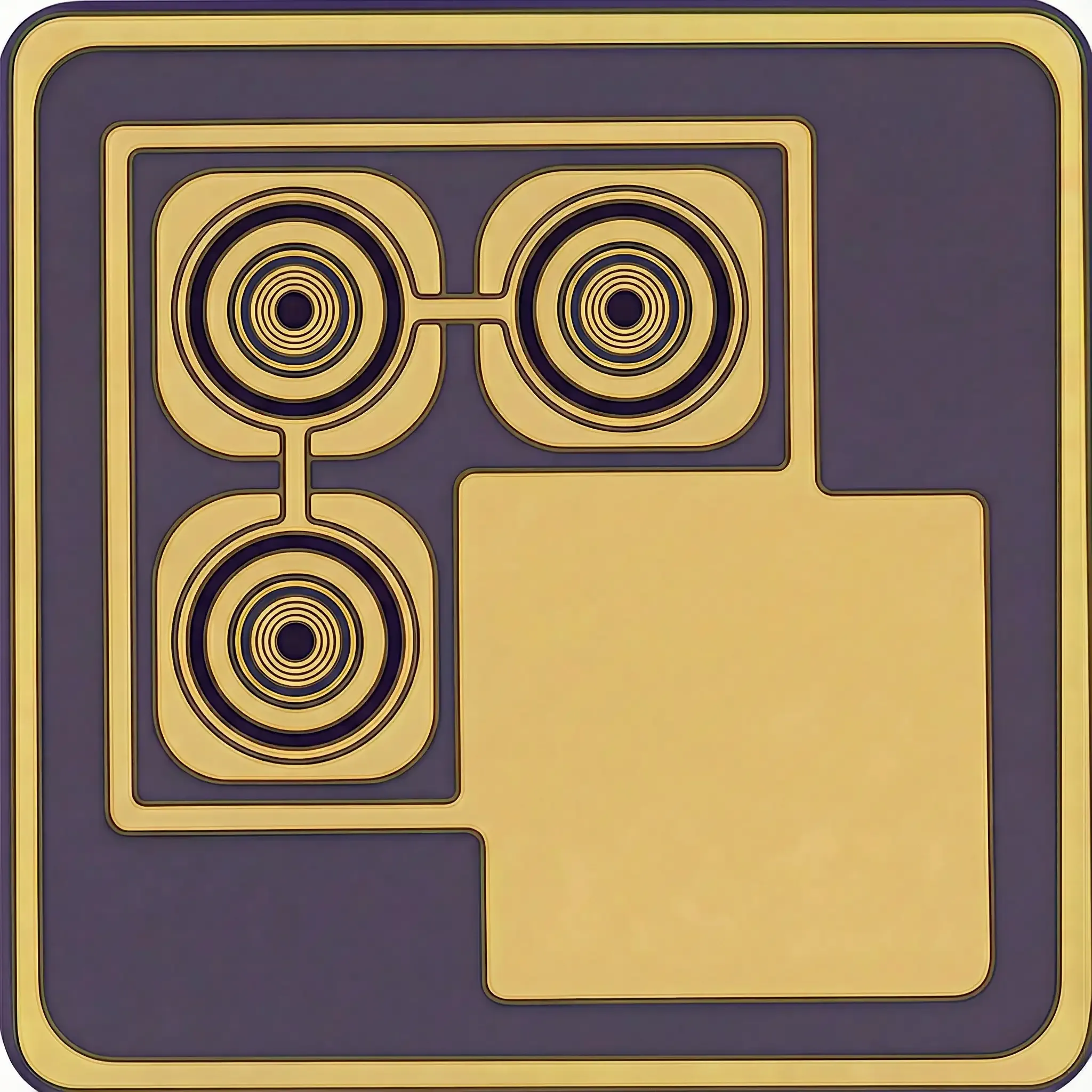
The 660nm 5mW VCSEL chip uses three emitters within an approximately 200μm square die.
It provides higher optical output than the 2mW model while maintaining a compact die footprint. The device is suitable for three-emitter VCSEL packaging, compact red-light modules and projects requiring a balance between optical output and chip area.
Packaging directions include custom ceramic packages, custom SMD package development, TO-can integration and optical-module assembly.
660nm 7mW VCSEL Bare Die
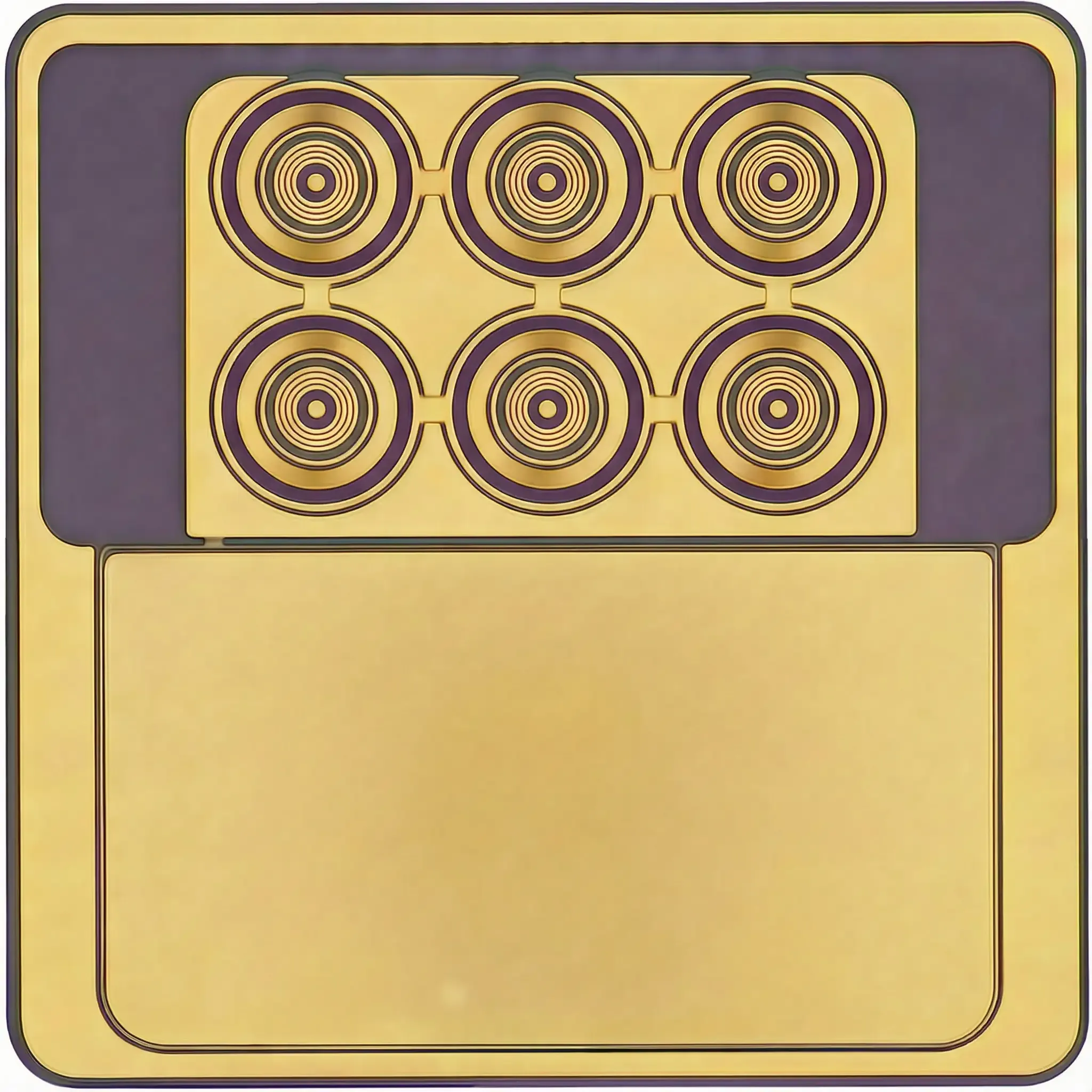
The 660nm 7mW VCSEL chip uses six emitters in a compact, non-square die measuring 163 ± 10μm × 185 ± 10μm.
This six-emitter 660nm VCSEL provides higher optical output under a 15mA test condition and is suitable for compact multi-emitter VCSEL packaging, higher-output visible-red modules, ceramic-submount integration and custom laser packages requiring increased emitter density.
3. Packaging, Optical Module and Application Development
OSAT and Custom VCSEL Packaging
The devices can be supplied as VCSEL die for packaging in wire-bonded ceramic-submount assemblies, custom SMD packages, TO-can packages, ceramic laser packages and application-specific optical modules.
Packaging and integration directions include:
- VCSEL die attach
- Gold-wire bonding
- Ceramic-submount assembly
- Custom VCSEL packaging
- Custom SMD laser packages
- TO-can laser packages
- Ceramic laser packages
- COB and compact optical-source modules
- Multi-emitter VCSEL modules
- Application-specific laser-device packages
The range of output powers and emitter configurations allows packaging companies to select a device according to package dimensions, bond-pad layout, optical-output requirements and module structure.
Lens and Beam-Shaping Integration
The series can also support optical lens, collimation and beam-shaping companies developing integrated laser-source assemblies.
Possible integration directions include:
- Collimation-lens assemblies
- Beam-shaping optical components
- Diffuser-integrated modules
- Lens-integrated VCSEL sources
- Compact visible-red optical assemblies
The 2mW, 5mW and 7mW models allow engineering teams to compare emitter layouts, far-field distribution, lens dimensions and module configurations.
Laser and Optical Module Development
The 660nm red VCSEL bare die series can be used in:
- Visible-red laser modules
- Sensor light sources
- Consumer-electronics light sources
- Machine-vision support illumination
- Alignment and indication systems
- Engineering and research light sources
- Custom optoelectronic modules
The corresponding datasheets identify sensor light sources, consumer electronics, machine vision and red lighting as application directions.
For customers who require completed surface-mount packages instead of bare die, 1ONELASER also provides the 660nm 5/7mW VCSEL SMD Series for SMT placement, reflow soldering and PCB-level integration.
The SMD series includes 5mW and 7mW visible-red VCSEL package options such as 2016, 2835, 3030 and 5730 packages for customers developing PCB-level red-light source products.
Medical Beauty and Red-Light Product Development
The series can also support beauty and personal-care prototypes, photobiomodulation-related optical development, hair-growth and scalp-light devices, and other projects requiring a 660nm visible-red source.
These are downstream applications after the VCSEL bare die has been integrated into an appropriate package or optical module. The primary focus of this page remains bare-die supply, packaging, wire bonding and module integration.
Distribution and Supply-Chain Support
The 660nm VCSEL Bare Die Series is also available to laser-component distributors, optical-module agents, technical sourcing companies and second-source development teams supporting customer packaging and integration projects.
Related Articles
4. Evaluation Kit and Documentation Support
The 660nm VCSEL Bare Die Series is available as an Evaluation Kit with 10 pcs / KIT for packaging trials, die-attach development, wire-bonding verification and initial optical integration.
Samples & Pilot Production: Evaluation kits, low-volume pilot production, and pre-production validation are supported.
- One selected model per kit: 2mW, 5mW or 7mW
- Corresponding product datasheet and die-dimension documentation
- International shipping quoted according to destination
- We offer project-specific configuration of center wavelength, wavelength tolerance, optical output power, power-bin selection and emitter-configuration requirements.
For component-level project evaluation, an Initial Product Report covering the Laser Diode Series and VCSEL Laser Diode Chip Series has been filed with the U.S. FDA CDRH. This filing supports technical documentation and product evaluation.
For applicable products, CE, EMC, EN 60825, LVD, RoHS, REACH and halogen-free certification and compliance documents are available. Documentation depends on the corresponding product model and does not represent certification of the customer's finished device.
5. Frequently Asked Questions
FAQ 1. What is the difference between the 2mW, 5mW and 7mW 660nm VCSEL bare die models?
The main differences are optical output power, emitter count, die dimensions and test current.
- The 2mW VCSEL chip uses a single emitter and a 200μm × 200μm die for low-power, single-emitter packaging.
- The 5mW VCSEL chip uses three emitters in an approximately 200μm square die for medium-output multi-emitter modules.
- The 7mW VCSEL chip uses six emitters in a 163 ± 10μm × 185 ± 10μm die for higher-output, compact multi-emitter packaging.
The appropriate model depends on the target optical output, available die space, emitter layout, package structure and module-integration requirements.
FAQ 2. What packaging methods are suitable for the 660nm VCSEL Bare Die Series?
The series can be used for VCSEL die attach, gold-wire bonding, ceramic-submount assembly, custom SMD packages, TO-can packages, ceramic packages and compact optical-module integration.
The unpackaged die must be integrated using an appropriate mounting, bonding, thermal-path and package design. 1ONELASER offers bare-die supply, power-bin selection, emitter configuration and custom VCSEL packaging according to project requirements.
FAQ 3. How is the 660nm VCSEL Bare Die Series different from the 660nm VCSEL SMD Series?
The 660nm VCSEL Bare Die Series supplies unpackaged VCSEL chips for OSAT providers, laser-packaging companies, die-attach and wire-bonding teams, ceramic-submount integrators and optical-module manufacturers.
The 660nm VCSEL SMD Series consists of completed surface-mount devices intended for SMT placement, reflow soldering and direct PCB integration.