
780nm
780nm 1W QCW VCSEL Bare Die
780nm 1W QCW VCSEL bare die with a 270-emitter array, 730 x 730um die and QCW drive for component-level NIR optical-source development.
Specifications
- Product Type
- Multi-mode VCSEL Bare Die
- Wavelength
- 780nm typ.; 774nm – 786nm
- Optical Output Power
- 0.95W min. / 1W typ.
- Emitter Configuration
- 270 emitters
- Operating Mode
- QCW; 10ms pulse width, 10% duty cycle
- Die Size
- 730 ±20μm × 730 ±20μm
- Recommended Assembly
- Die Attach / Wire Bonding / Ceramic Submount / Custom Packaging
1. 780nm 1W QCW VCSEL Bare Die for Component-Level NIR Source Development
The 780nm 1W QCW VCSEL bare die is a multi-emitter semiconductor laser chip for pulsed near-infrared optical-source development. It is supplied as an unpackaged die for die attach, wire bonding and custom packaging.
The released electro-optical table specifies 0.95W minimum and 1W typical optical output at an operating current of 1.2A, under QCW testing with a 10ms pulse width, a 10% duty cycle and a 25 °C heat-sink temperature. The die contains 270 emitters in a 730 ±20μm × 730 ±20μm structure with a 100 ±15μm thickness.
Typical development directions include pulsed NIR illumination sources, industrial optical sensing, machine-vision light sources, optical measurement and custom packaged laser modules. The die is an engineering component; final performance depends on die attach, wire bonding, thermal path and package design.
For application-level source selection, visit the Sensing & Machine Vision solution page. To compare the complete 780nm product range, view the 780nm VCSEL SMD Series.
Lead Time: In-stock products are dispatched within 3 business days; custom-packaged products have a lead time of 15–20 days.
MOQ: The minimum order quantity is 1 reel; selected special models support small-batch orders.
2. Optical and Electrical Characteristics
The values below follow the released datasheet. Unless otherwise stated, all tests are performed under QCW conditions with a 10ms pulse width, a 10% duty cycle and a 25 °C heat-sink temperature.
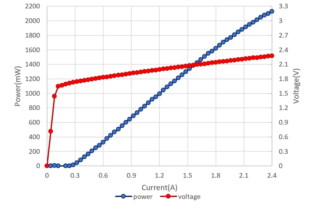
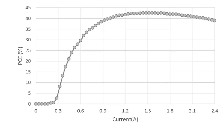
Full electro-optical data, typical LIV curves and power-conversion-efficiency curves are provided in the product datasheet, available in the Documentation Support section below.
The published typical values are internally consistent at the operating point: 1W output at 1.2A and 2V corresponds to the specified 42% typical power conversion efficiency.
The datasheet slope-efficiency and threshold-current entries should be read together with the typical LIV curve; contact 1ONELASER for model-specific binning data.
3. Application, Packaging and Integration Notes
Component-Level Integration
The die is intended for customers who assemble their own optical sources. Die attach, wire bonding, package protection and thermal management are defined by the module design.
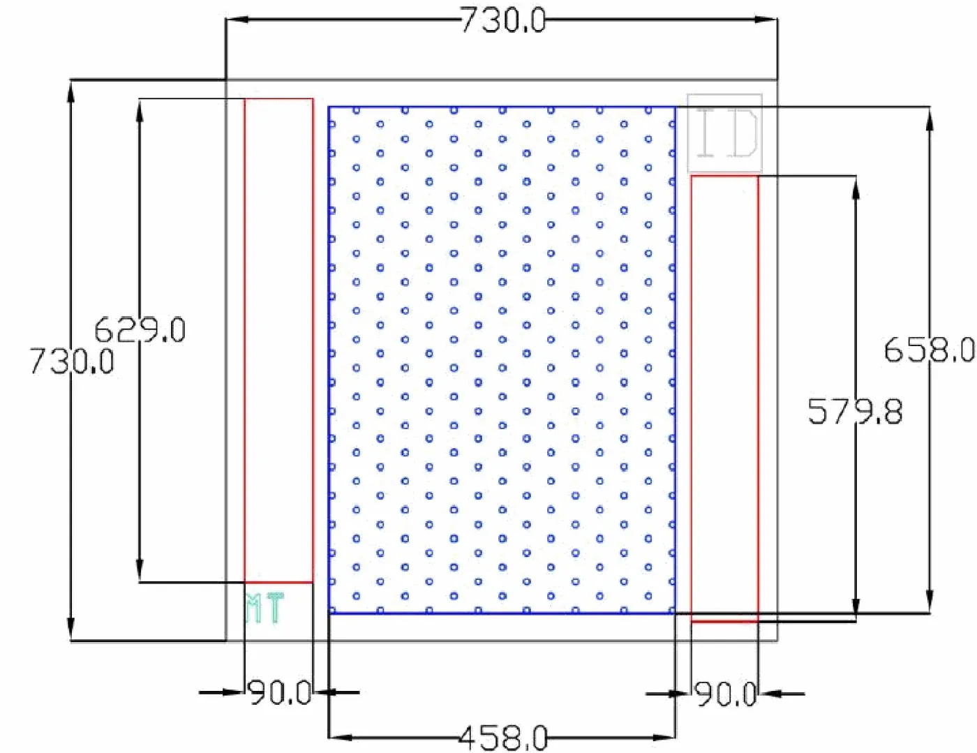
Bond-pad geometry and electrode arrangement are shown in the datasheet mechanical drawing. Both the anode contact on the emission side and the backside cathode contact use gold surfaces.
Pulsed Drive Conditions
The device is specified for QCW operation. The 10ms pulse width and 10% duty cycle values are the standard test conditions and do not define the absolute maximum ratings of the device.
Drive electronics should provide controlled pulse timing, stable peak current and protection against overshoot. Thermal design should account for the average power at the selected duty cycle.
Quality and Compliance
The datasheet provides RoHS and REACH compliance statements and handling guidance. ESD precautions are required during storage, die handling, assembly and testing.
For applicable products, CE, EMC, EN 60825, LVD, RoHS, REACH and halogen-free certification and compliance documents are available. Documentation depends on the final model and configuration.
Related Articles
4. Evaluation Kit and Documentation Support
The 780nm 1W QCW VCSEL bare die supports die attachment, wire bonding, driver development, thermal validation and optical integration.
An Evaluation Kit with 10 pcs / KIT is available for electrical, thermal and optical assessment under project-specific test conditions.
Samples & Pilot Production: Evaluation kits, low-volume pilot production, and pre-production validation are supported.
We offer project-specific support for operating mode, optical output requirement, drive current, pulse width and duty cycle, die and bond-pad structure, ceramic-submount integration, thermal-path development and custom packaging.
5. Frequently Asked Questions
FAQ 1. What are the specified operating conditions of the 780nm 1W QCW VCSEL bare die?
The released table specifies 0.95W minimum and 1W typical optical output at 1.2A with a typical operating voltage of 2V, under QCW conditions with a 10ms pulse width, a 10% duty cycle and a 25 °C heat-sink temperature.
FAQ 2. How many emitters does the die contain and what is its size?
The die contains 270 emitters in a 730 ±20μm × 730 ±20μm chip with a 100 ±15μm thickness. The emission-side anode and backside cathode use gold contact surfaces.
FAQ 3. Can the 780nm 1W die be operated continuously?
The device is specified under QCW conditions. Continuous-wave operation is not covered by the released ratings and would require separate engineering validation of the die, package and thermal path before use.