
Oct 6, 2026Technical Insights
660nm Red Light Sources for Devices — 5mW or 7mW?
660nm red light sources for therapy and beauty devices: choosing 5mW vs 7mW, emitter pitch, irradiance and dose, and SMD packages.
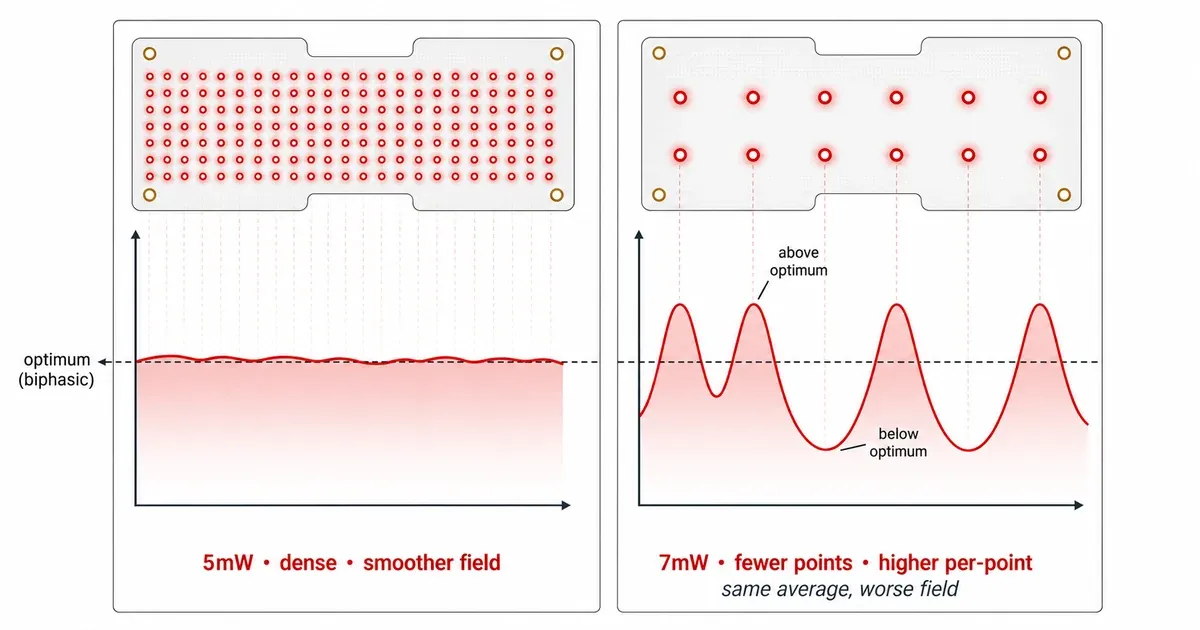
Choosing a 660nm red light source is not a matter of buying the highest power. It is matching power class, package, and beam to your emitter count, working distance, and treated area. A 5mW part spread across many points often produces a better field than a 7mW part in fewer positions, and the published dose-response data explains why. Photobiomodulation has an optimum, and past it the reported effect falls away. This article gives the arithmetic behind the choice: irradiance, dose, emitter pitch, and thermal load, so it is calculated rather than argued.
Why 660nm, in one line
660nm is the most commonly selected red wavelength for skin, scalp, and other superficial applications, and the most studied of the red band. Reported effects across 630nm – 670nm are broadly similar, which does not make those wavelengths interchangeable for a given application. In photobiomodulation research the absorber itself is still debated: cytochrome c oxidase is the most widely discussed candidate, and the evidence has been challenged. None of that changes the arithmetic below. Which wavelength to pick across the red band, and when a design needs near-infrared as well, is covered in our wavelength selection guide. This article assumes 660nm is set and looks at choosing the right 660nm part.
More optical power is not automatically better
PBM does not scale linearly with light. The literature describes a biphasic dose response: too little light does little, and past an optimum the effect falls away again. More light is not more result.
Harder still for a hardware team, irradiance matters independently of total dose. The same review describes a 660nm animal study in which two groups received an identical 0.9 J/cm² per point, one at 55 mW/cm² over 16 seconds and the other at 155 mW/cm² over 6 seconds. The lower-irradiance group showed a measurable improvement; the higher-irradiance group was not significantly different from untreated controls. Same wavelength, same dose, different outcome, because the rate of delivery changed.
For an emitter decision that means per-point optical power is a variable to land on target, not a number to maximize. That is the engineering case for taking 5mW seriously.
What actually changes between 5mW and 7mW
On the 660nm VCSEL SMD series, the 5mW class runs about 5.0–5.5mW typical and the 7mW class about 7.0mW typical, both at IF = 10mA. Because drive current and forward voltage are comparable, the electrical load per emitter is roughly the same either way, and the 7mW part simply converts more of it into light. Per emitter, 7mW is the more efficient point.
The trade is not efficiency. It is how a total gets spread:
- 5mW: a denser array, more overlap between neighboring spots, less optical energy at each point on the skin, and a smoother field. Offered in 2016, 2835, and 5730.
- 7mW: more output per position, or the same total from fewer parts and a simpler board. Offered in 2016, 2835, 3030, and 5730. Pitch and optics have to work harder to keep the field even.
Given a biphasic response, the peaks in that field matter as much as the average. A sparse array of brighter points can sit above the optimum directly under each emitter and below it in between, while the averaged number on your report looks correct.
How to calculate irradiance and dose for a 660nm array
Start from the array, not the component. Four steps, with one worked example to replace with your own numbers:
- Total optical output = emitter count × per-emitter output. 120 × 5mW = 600mW.
- Average irradiance = total output ÷ treated area. 600mW ÷ 200cm² = 3 mW/cm², before optical losses and before distance and overlap effects.
- Dose = irradiance × exposure time. 3 mW/cm² × 600s = 1.8 J/cm².
- Duty cycle for a QCW mode: average optical power = peak × duty. At 10% duty that 1.8 J/cm² becomes 0.18 J/cm² over the same wall-clock time.
As a sanity check on the arithmetic only, the review above puts fluences commonly used in research at roughly 1–20 J/cm², with irradiances around 5–50 mW/cm² for stimulation and healing. Those are research ranges, not a protocol: your dose target, exposure plan, and validation are yours to set and own.
If the number lands short, note which lever is actually large. Moving from 5mW to 7mW adds about 40% to the total. Doubling the emitter count adds 100%. Tightening the treated area or the working distance can beat both. The higher-power part is one term in the equation, and rarely the biggest one.
Emitter pitch and the donut beam
Multimode VCSEL designs, including the parts in this series, can produce an annular, donut-shaped far field with reduced intensity near the optical axis. A single emitter is therefore not uniform on its own, and no amount of binning makes it so. The array creates the even field, and the geometry is simple:
spot diameter ≈ 2 × working distance × tan(divergence ÷ 2)
At the 18°–20° typical divergence of these 660nm SMD parts:
Working distance | Spot diameter (18°–20°) |
|---|---|
5mm | ~1.6–1.8mm |
10mm | ~3.2–3.5mm |
20mm | ~6.3–7.1mm |
30mm | ~9.5–10.6mm |
Set the emitter pitch at or below the spot diameter at your working distance and neighboring donuts overlap, each one filling its neighbor’s dim center. Space them wider and the treated field becomes a pattern of rings. A diffuser or micro-lens array can rescue a layout that cannot get the pitch down, at the cost of some output.
One caveat before building to these numbers: divergence can be quoted as a full angle or a half angle, at 1/e² or at FWHM. The table assumes 18°–20° is the full angle. Confirm the definition on the model datasheet, because a factor-of-two error here reaches the lab as a striped mask.
Package, drive current, and thermal budget
Package choice follows PCB area, the pitch you just calculated, product thickness, and thermal path. The series offers 2016 (2.2 × 1.6mm) for compact, wearable, and high-density boards; 2835 (3.5 × 2.8mm) for standard SMT; 3030 (3.0 × 3.0mm) for 7mW and balanced mechanical designs; and 5730 (5.7 × 3.0mm) for a larger pad area.
The driver is designed around a threshold current of roughly 1.5–4.0mA and a forward voltage of 2.3–2.6V at 10mA, run as constant current.
Then do the thermal sum, because it is usually the number that bites. At 2.3–2.6V and 10mA each emitter draws roughly 23–26mW of electrical power and converts 5–7mW of it into light. The remainder, approximately 16–21mW per emitter depending on the model and operating point, becomes heat in the package and the board. A 120-emitter array is therefore pushing on the order of 2.4W into the PCB, continuously in CW. That figure, not the optical rating, sizes copper pour, board material, and enclosure venting. QCW at a low duty cycle scales it down proportionally.
Consistency across a production run
A device that has to pass validation and satisfy brand or clinical partners needs units that behave alike. Wavelength binning keeps every unit on the same part of the absorption curve. Tolerance on this series is specified per model rather than as one published figure across the range, and center wavelength, tolerance, and power bin can all be specified per project. Power binning keeps optical output aligned across a batch.
Threshold current and forward voltage matter for the same reason. A constant-current driver set for one batch will produce different optical output from a batch whose threshold has shifted, and that drift lands in the measured output of the finished device, which is what gets flagged in validation or by a demanding buyer. Set against the cost of a rebuild, a tight bin is cheap insurance.
SMD or bare die for 660nm
If your team places finished parts with pick-and-place equipment, as most brands and circuit-design houses do, the SMD series drops onto the board directly. If you build your own package or module, as OSAT providers, laser-packaging companies, and ceramic-submount integrators do, the 660nm bare die in 5mW and 7mW leaves die attach, wire bonding, and submount assembly to you. The full make-or-buy decision is its own topic; the short version is that it follows your team’s assembly capability and volume, not the price of the part.
The component boundary, and what to settle before you commit
The 660nm VCSEL is a component-level light source. The finished-device manufacturer remains responsible for optical-dose validation, laser-safety classification, applicable photobiological risk assessment, product testing, labeling, and any medical, beauty, or veterinary claim. Standards such as EN 60825-1 may be relevant to laser product classification depending on the finished product and jurisdiction. A supplier provides the source and its specifications, not therapeutic performance. One scope note belongs here too: for deeper targets such as joints, tendons, and many pet and equine applications, 660nm alone does not reach far enough, and a combination such as 660nm and 850nm should be evaluated, as noted on our medical beauty and personal care page.
Then the practical part, and it is the same for every team that builds one of these. Every number above is a number at the emitter, worked on paper. The field your device actually delivers depends on your pitch, your working distance, your optics, and your enclosure, and none of that is on a datasheet. So the usual sequence is to build a small pilot array and measure the field before committing a layout, rather than discovering it after tooling. Evaluation kits are one practical route to that: 10 pieces, with power class and package chosen for the design in question. Documentation support sits alongside it where a design file needs it, including an Initial Product Report filed with the U.S. FDA CDRH for the laser diode and VCSEL chip series, and CE, EN 60825, RoHS, REACH, and halogen-free documents per model. That is the kind of project 1ONELASER typically supports.
FAQ
Is 7mW better than 5mW for a 660nm red light therapy device?
Not automatically. At the same 10mA drive the two draw similar electrical power, so 7mW is the more efficient point. But PBM has a biphasic dose response, and a sparse array of brighter points can overshoot under each emitter and undershoot between them. For masks and caps with many evenly spaced sources, 5mW often gives the smoother field; 7mW suits fewer sources or more output per position.
How do I calculate irradiance and dose for a 660nm array?
Total output = emitter count × per-emitter mW. Average irradiance = total output ÷ treated area. Dose = irradiance × exposure time. For QCW, average power = peak × duty cycle. Example: 120 × 5mW = 600mW over 200cm² = 3 mW/cm²; over 600s that is 1.8 J/cm², before optical losses.
What emitter pitch should I use?
Spot diameter ≈ 2 × working distance × tan(divergence ÷ 2). At 18°–20° divergence and a 10mm working distance that is roughly 3.2–3.5mm, so a pitch at or below about 3mm lets neighboring donut spots overlap. Confirm whether the datasheet quotes full or half angle before building to it.
What packages does the 660nm SMD come in?
Four: 2016 (2.2 × 1.6mm), 2835 (3.5 × 2.8mm), 3030 (3.0 × 3.0mm), and 5730 (5.7 × 3.0mm). The 5mW class is offered in 2016, 2835, and 5730; the 7mW class adds 3030.
Is the 660nm source CW or pulsed?
Both, CW or QCW, depending on the model. Duty cycle scales both delivered dose and thermal load, so confirm the operating mode against your driver and exposure plan before design-in.
How consistent is the wavelength across units?
660nm typical, with tolerance specified per model rather than as one figure across the series. Center wavelength, tolerance, and power bin can be specified per project. A tight bin keeps every unit on the same part of the absorption curve, so device output stays consistent batch to batch.
Do I need 850nm as well as 660nm?
For surface targets, no. For joints, tendons, or deeper tissue, including many pet and equine applications, 660nm does not penetrate far enough on its own, and a red plus near-infrared combination such as 660nm and 850nm should be evaluated.
Choose the 660nm part from your treated area and emitter count, calculate irradiance and dose before selecting a power class, set pitch from the divergence, and budget the waste heat. 1ONELASER develops 660nm red light-source solutions in 5mW and 7mW SMD and bare die, with custom package and array options where a catalog part cannot meet the pitch or tolerance a design needs.