
Oct 24, 2026Technical Insights
VCSEL vs Edge Emitting Laser Which Should You Use
Choose between a VCSEL and an edge emitting laser by matching beam geometry, wavelength behavior, single-emitter power, array needs, manufacturability, and system cost to the real application.
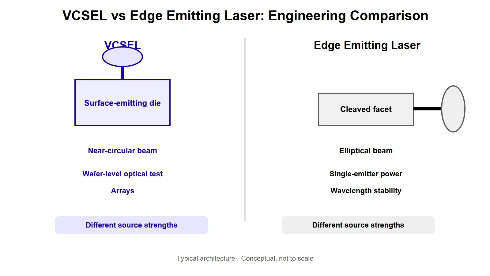
Choose a VCSEL when your design benefits from a more symmetric native beam, surface-normal emission, wafer-level optical testing, two-dimensional arrays, compact parallel emitters, or relatively stable cavity-defined wavelength behavior.
Choose an edge emitting laser when the application needs high optical power from one stripe, a mature high-power diode architecture, a side-emitting geometry that already fits the optical path, or a wavelength and package ecosystem better served by conventional laser diodes.
Neither is the premium version of the other.
The useful decision is which architecture creates less optical, thermal, manufacturing, and calibration work at the required system performance.
Requirement | VCSEL | Edge Emitting Laser |
|---|---|---|
Native beam | Often more symmetric | Often elliptical with different fast and slow axis divergence |
Emission direction | Normal to wafer surface | From a cleaved chip edge |
Wafer-level optical test | Practical before dicing | Final optical cavity generally requires cleaving first |
2D monolithic arrays | Natural architecture | Not the usual monolithic scaling path |
High power from one emitter | More constrained | Often stronger choice |
Power conversion efficiency | Strongly device and wavelength dependent | Strongly device and wavelength dependent |
Wavelength temperature behavior | Often lower drift because cavity resonance sets wavelength | Often more tied to gain peak and can drift more with temperature |
Facet processing | No cleaved output facet | Cleaved and coated output facets are central to the device |
Beam shaping need | Can be simpler for circular spots, but mode structure still matters | Often needs fast and slow axis correction for a symmetric spot |
Cost | Can benefit from wafer-level testing and arrays at volume | Can be economical for mature single-emitter products |
Best choice | Depends on system requirement | Depends on system requirement |
If you need a structure-level refresher before comparing the two architectures, start with what a VCSEL is.
Beam shape is usually the first visible difference
An edge emitting laser confines light in an asymmetric waveguide.
Because the vertical and lateral mode dimensions are different, the emitted beam commonly has different divergence in the fast and slow axes. The result is often an elliptical beam that may need additional optics if the application needs a round or uniformly filled spot.
A VCSEL emits perpendicular to the wafer surface. The aperture geometry is more symmetric, so the native beam is often closer to circular.
Edge emitters commonly show substantially different fast-axis and slow-axis divergence, while VCSELs often provide a more symmetric angular distribution. Compare only values measured with the same divergence definition, such as FWHM or 1/e² full angle.
A technical review of single-mode photonic-crystal VCSELs notes three manufacturing and optical features that distinguish the architecture from edge emitters: circular output beams, wafer-level testing, and the ability to form two-dimensional arrays.
That does not mean every VCSEL produces a perfect Gaussian spot.
Multimode operation, current crowding, aperture size, emitter layout, package optics, and thermal gradients can all change the far field.
The correct comparison is therefore:
What beam reaches the target after the complete optical system?
Measure the spot, divergence, uniformity, and usable optical power after the lens or diffuser you actually plan to ship.
An edge emitter can still be the easier path when one strong beam is needed
A common mistake in VCSEL comparisons is to focus on array scalability and forget that many applications do not need an array.
If the product needs one relatively high-power semiconductor laser stripe coupled into an optical system, an edge emitter may be the more direct architecture.
A recent Laser & Photonics Reviews article summarizes the traditional tradeoff clearly: edge emitting lasers can provide high optical output but often with an elliptical beam, while VCSELs provide more circular low-divergence emission but are more constrained in single-mode power.
Power-conversion efficiency should be compared at the required wavelength, output level, pulse condition, and temperature. Mature high-power edge emitters can achieve very high efficiency, while modern VCSEL arrays can also reach competitive values. Architecture alone is not enough to predict the winner.
The exact power boundary depends on wavelength, stripe or aperture geometry, operating mode, package, thermal design, and required beam quality, so there is no universal mW or W threshold where one architecture automatically becomes better.
Start from the target:
- required optical power at the target
- spot size
- beam shape
- working distance
- pulse duration
- duty cycle
- thermal limit
- package size
Then determine which emitter reaches that point with the simpler optical train.
VCSEL arrays change how power can be scaled
VCSELs can scale total output by placing many apertures on the same surface-emitting die.
This is fundamentally different from asking one aperture to carry all of the optical load.
For illumination, sensing, heating, and other array-based applications, the engineer can distribute emitters across a defined layout and then use optics to combine or reshape the field.
That gives the design team control over:
- emitter count
- pitch
- active area
- electrical grouping
- beam overlap
- illumination footprint
- local current density
But arrays introduce their own limits.
As emitter count and current increase, current distribution, thermal gradients, optical nonuniformity, and mode behavior become more difficult to control.
So the correct statement is not that VCSELs scale power easily.
The more useful statement is:
VCSELs provide a natural two-dimensional path for distributing optical output across many surface emitters.
Whether that is better than one or more edge emitters depends on the required field.
Wavelength stability is an important difference in temperature-sensitive systems
In many VCSELs, the lasing wavelength is strongly influenced by the short optical cavity resonance.
In conventional edge emitting lasers, the operating wavelength is more closely tied to the semiconductor gain spectrum and longitudinal modes of the longer cavity.
That architectural difference often gives VCSELs a lower wavelength temperature coefficient than comparable edge emitting laser diodes.
RP Photonics notes that GaAs-based VCSEL arrays commonly show cavity-defined wavelength temperature behavior and that the temperature dependence can be several times lower than for edge emitting laser diodes.
Do not convert that into a universal number for every product.
Actual drift depends on:
- material system
- wavelength
- cavity design
- current
- thermal resistance
- pulse condition
- junction temperature
- mode behavior
The practical benefit appears only when the application is wavelength sensitive.
Examples include systems with narrow optical filters, spectroscopy-adjacent sensing, atomic or molecular interactions, and receivers whose responsivity changes strongly with wavelength.
For a simple red-dot indicator, a small wavelength shift may not matter at all.
Manufacturing architecture is one of the strongest VCSEL differences
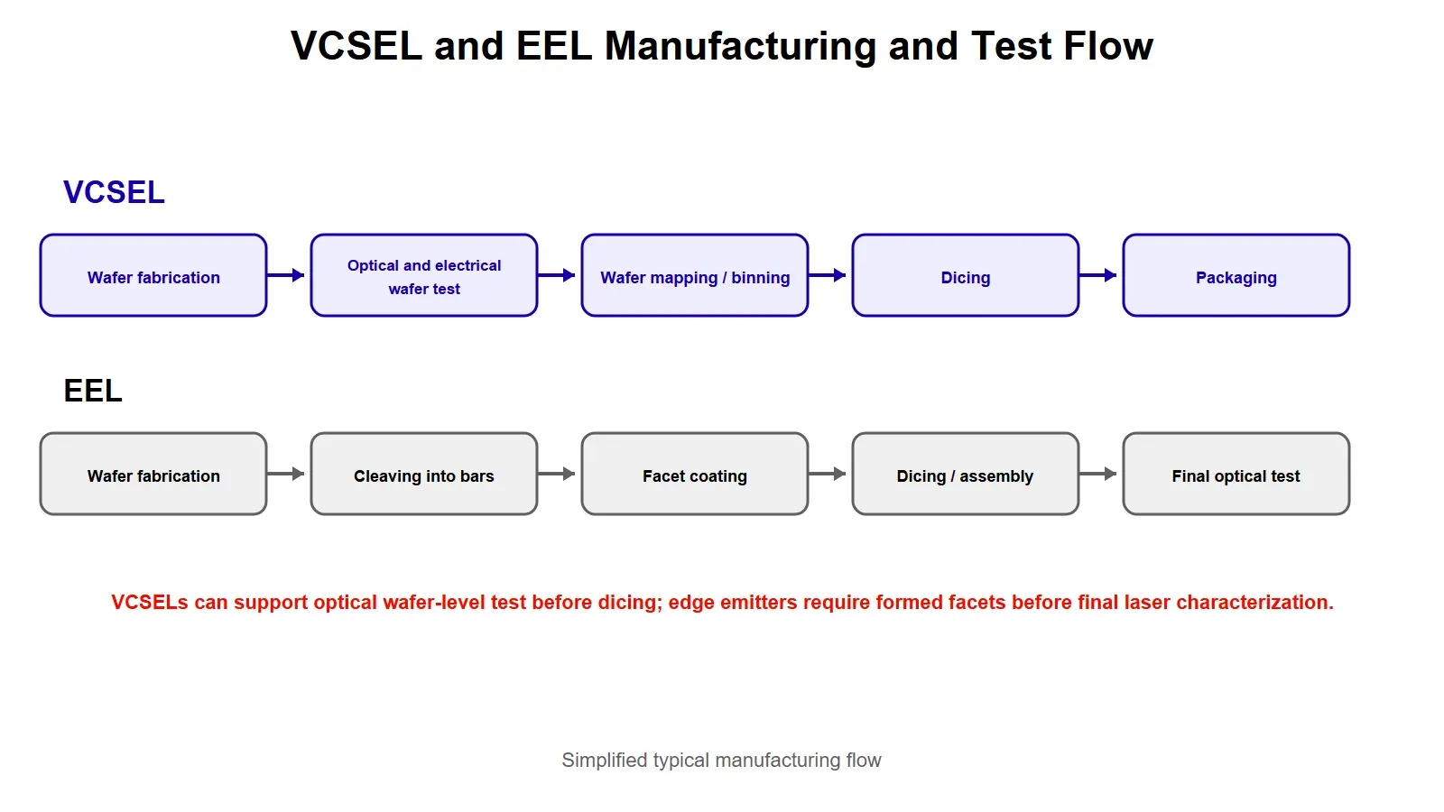
Both VCSELs and edge emitting lasers begin with wafer fabrication.
The difference is when the optical cavity becomes complete enough to test.
A VCSEL is surface emitting, so the processed device can be electrically and optically characterized while it is still on the wafer. Off-spec dies can be identified before dicing and final packaging.
An edge emitting laser relies on cleaved facets that become part of the optical cavity. Final optical testing therefore follows the cleaving step.
Laser Focus World describes this distinction as a major manufacturing advantage of VCSELs because wafer-level testing can remove bad dies earlier and reduce downstream testing and packaging cost.
This matters most at volume.
It can support:
- automated wafer mapping
- optical binning
- earlier removal of bad dies
- tighter production population control
- more efficient selection for array assembly
But it does not mean every VCSEL is cheaper than every edge emitter.
Unit cost still depends on epitaxy, yield, wavelength, die area, package, optics, power, test limits, order volume, and supplier process maturity.
Use the manufacturing architecture to understand where cost can be removed, not to invent a universal price rule.
Edge emitters carry a facet process that VCSELs do not
The output facet of an edge emitting laser is formed by cleaving the semiconductor and usually requires controlled coating and passivation.
This facet operates at high optical intensity and can become a reliability-critical part of the device.
Photonics Spectra describes edge emitter production as including wafer cleaving, facet coating, bar handling, and later device testing. The same source discusses catastrophic optical damage as a facet-related failure mechanism that has to be controlled in high-power edge emitters.
VCSELs avoid the same cleaved output-facet architecture because the optical field exits through the wafer surface.
That avoids the same cleaved-output-facet failure path, but it does not make VCSELs immune to optical or reliability failures.
VCSEL reliability still depends on:
- junction temperature
- current density
- oxide aperture stress
- metallization
- ESD
- package stress
- moisture control
- bond quality
- array current sharing
Compare the actual reliability data for the candidate parts under the intended operating condition.
Beam correction optics can change the total system cost
A low-cost emitter is not always the low-cost optical system.
An edge emitting laser with a strongly asymmetric fast and slow axis may need:
- aspheric collimation
- cylindrical optics
- fast-axis correction
- slow-axis correction
- careful rotational alignment
A VCSEL with a sufficiently symmetric beam may need fewer beam-correction elements in an application that only needs a round spot.
But this is not guaranteed.
A multimode VCSEL array that produces a ring-shaped or structured far field may still need a diffuser, microlens array, homogenizer, or custom beam-shaping optic.
A practical cost model is:
system source cost = emitter + driver + optics + alignment + thermal path + assembly + calibration + test
That is the number that should drive the architecture decision.
Why some VCSELs can produce a filled or solid spot
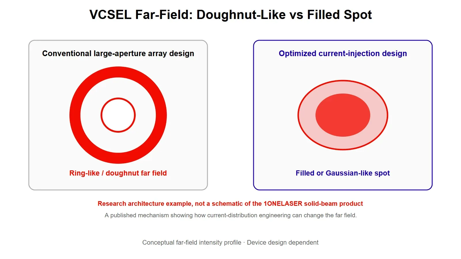
A high-power VCSEL array does not automatically produce a filled spot.
Large apertures and high current can create current crowding near the edge of the active region. That can favor higher-order modes and produce a doughnut-like far field.
A 2026 Optics & Laser Technology paper on a large-aperture VCSEL array described exactly this problem. The researchers used a center vertical injection design to reshape the current distribution and reported a superior Gaussian-shaped beam compared with the conventional edge-crowded pattern.
That is an important engineering distinction.
A filled or solid beam is a device-design result, not a generic property of the VCSEL category.
1ONELASER currently lists an 808nm Solid-Beam VCSEL Series with 3 W and 8.2 W typical model options under the source-stated QCW condition of 0.3 ms pulse width and 1% duty cycle. The product page specifies 808 nm typical wavelength and separate emitter counts for the two dies.
Those numbers apply only to that series and its stated test conditions.
They should not be generalized into a claim that all 808 nm VCSELs produce the same spot or that every solid-beam architecture is Gaussian under every current and temperature.
For a project that needs a filled spot, ask the supplier for the actual near-field and far-field data at the intended operating point.
A solid spot requirement should be written as a measurable optical specification
The words solid beam or solid spot are too vague for an engineering drawing.
Define the target using measurable conditions such as:
1. working distance
2. target plane
3. spot width or diameter
4. beam divergence definition
5. irradiance uniformity
6. center-to-edge ratio
7. allowable central depression
8. allowed hot spots
9. pulse width and duty cycle
10. drive current
11. source temperature
12. lens or diffuser configuration
If the application is thermal or skin facing, also define the acceptable peak irradiance and spatial distribution at the target.
A beam image with no operating condition is not enough.
For custom spot-size, diffuser, collimation, and coupling discussions, 1ONELASER's Custom Laser Source Development path covers wafer-level optics, collimation, diffusers, coupling optics, and module-level integration.
Edge emitters can be the better choice for focused point projection
VCSEL advantages are strongest when surface emission, arrays, compact packaging, or production testability solve a real problem.
A simple point-projection system may not need any of those advantages.
An edge emitting laser module with an adjustable lens can be a practical source when the design needs:
- a visible red point
- adjustable focus
- a known side-emitting diode module architecture
- low optical power
- simple mechanical alignment
For example, 1ONELASER currently offers a 650nm adjustable-focus EEL module for red-dot projection and OEM integration.
That product is not a proof that edge emitters are better for all visible-laser applications. It is an example of the opposite of technology-first selection: when a conventional EEL module already matches the optical function, replacing it with a VCSEL may create unnecessary redesign.
VCSELs are often the stronger starting point for dense sensing arrays
A surface-emitting architecture becomes especially attractive when the product needs many optical emitters in a small footprint.
Examples include:
- structured or flood illumination
- short-range 3D sensing
- machine-vision illumination
- multi-zone optical sensing
- compact NIR emitter arrays
- array-driven beam shaping
Photolithographic placement allows emitters to be arranged directly on the die with a defined pitch.
This reduces the assembly burden compared with individually placing many discrete edge emitters.
The resulting system still has to control:
- current matching
- thermal gradients
- emitter failures
- optical uniformity
- diffuser or lens alignment
- detector field of view
For these applications, the Sensing and Machine Vision path is a useful starting point for source-level evaluation.
The wavelength requirement may decide the architecture before beam shape does
VCSEL and edge emitter availability is not identical across every wavelength and power range.
A system may have an ideal beam preference but still need to choose the architecture that has a mature source at the required wavelength.
This is common when the application needs:
- a telecom wavelength
- a specialized visible wavelength
- very high single-emitter power
- a particular package
- a source that already has established reliability data
Do not choose the architecture first and force the wavelength second.
Lock the required wavelength and tolerance, then compare the available VCSEL and edge emitter options that can actually meet it.
Use this decision sequence before selecting the laser
1. Lock the target-plane requirement
Define optical power, spot shape, working distance, divergence, uniformity, and pulse condition at the point where the light is used.
2. Decide whether you need one emitter or an array
If one strong beam solves the problem, an edge emitter may be simpler. If the field is naturally distributed across many emitters, VCSEL arrays deserve early evaluation.
3. Quantify beam-shaping work
List every lens, cylindrical optic, diffuser, homogenizer, and alignment step required by each source.
4. Define wavelength behavior
Specify center wavelength, tolerance, spectral width, and allowable drift with current and temperature.
5. Define the operating envelope
State CW, QCW, or pulse operation, peak current, pulse width, duty cycle, ambient temperature, and thermal path.
6. Compare manufacturing and test flow
For volume products, ask whether wafer-level binning, early screening, array integration, and automated optical test reduce downstream cost.
7. Compare total system cost
Include source, driver, optics, alignment, cooling, package, assembly, calibration, test, and expected yield.
8. Test both architectures where the decision is still close
Use the same target-plane measurement setup for both candidates.
The architecture that wins on the bench should win because it meets a measured system requirement, not because one technology has a longer list of generic advantages.
About 1ONEVCSEL
1ONEVCSEL is 1ONELASER's specialized product brand focused on VCSEL technology. Its current product and development paths include single-mode and multimode VCSELs, high-power arrays, 808 nm solid-beam VCSEL dies, SMD packages, and custom beam-shaping discussions. 1ONELASER's broader laser-source portfolio also includes selected EEL module projects.
For a VCSEL vs EEL evaluation, send the target wavelength, target-plane optical power, working distance, beam shape, spot size, operating mode, pulse condition, package limit, thermal constraint, and expected production volume.
We can then determine whether an available standard component is suitable or whether the project needs a custom wafer, package, optical, or module path.
Start with Request Evaluation Kits for component comparison or use Custom Development and ODM for a project-specific source.
The finished-device manufacturer remains responsible for optical safety, system reliability, regulatory compliance, performance validation, and final application claims.
Frequently asked questions
Is a VCSEL always cheaper than an edge emitting laser
No. VCSEL manufacturing can benefit from wafer-level optical testing and monolithic arrays, but actual component and system cost depends on wavelength, die size, power, package, optics, yield, order volume, and required testing.
Which has the better beam
A VCSEL often has a more symmetric native beam, while an edge emitter commonly has different fast and slow axis divergence. The better source is the one that produces the required target-plane beam after the complete optical system.
Which can produce more power from one emitter
Edge emitting lasers are often the stronger choice when high optical power is required from one stripe. VCSELs can scale total output through multiple surface emitters and arrays, but array thermal and uniformity limits still apply.
Are VCSEL wavelengths more stable with temperature
Often, yes, because the VCSEL wavelength is strongly determined by the short cavity resonance. The actual temperature coefficient still depends on the specific device and must be verified under the intended current and thermal condition.
Why can VCSELs be tested before dicing
The optical cavity and emitting surface are available on the processed wafer, so electrical and optical characterization can be performed before the wafer is diced. Edge emitters generally need cleaved facets before final laser operation can be tested.
Can a VCSEL produce a solid spot instead of a doughnut beam
Some VCSEL designs can. A filled or Gaussian-like beam depends on current injection, aperture design, mode control, emitter layout, optics, and operating point. It is not a universal VCSEL property.
When should I choose an edge emitting laser
Choose an EEL when a high-power single emitter, established point-projection module, mature wavelength ecosystem, or existing optical path makes the side-emitting architecture simpler and lower risk.
When should I choose a VCSEL
Choose a VCSEL when surface-normal emission, symmetric beam geometry, wafer-level testability, compact arrays, wavelength behavior, or multi-emitter integration removes a real system constraint.