
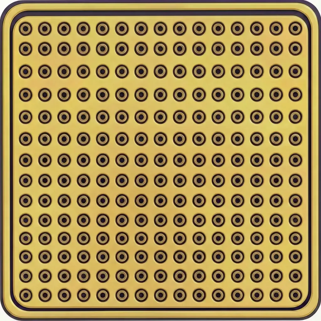
850nm
850nm 2W CW & QCW VCSEL Bare Die
850nm 2W CW and QCW VCSEL Bare Die with two separate multi-emitter NIR die options for continuous-wave, pulsed operation and OEM optical modules.
Specifications
- Product Type
- Multi-mode VCSEL Bare Die
- Wavelength
- 850nm typ.; 840nm – 860nm
- Optical Output Power
- CW: 1.9W min. / 2.1W typ.; QCW: 2.0W min. / 2.2W typ.
- Emitter Configuration
- Multi-emitter VCSEL arrays; QCW: 410 emitters; CW: not specified in the current datasheet
- Operating Mode
- CW / QCW, depending on model
- Die Size
- 1080 ±10μm × 1050 ±10μm / 995μm × 1020μm
- Recommended Assembly
- Die Attach / Wire Bonding / Ceramic Submount / Custom Packaging
1. 850nm 2W CW & QCW VCSEL Bare Die for Packaging and Module Integration
The 850nm 2W CW & QCW VCSEL Bare Die product page includes two separate multi-emitter near-infrared VCSEL die options for continuous-wave and pulsed optical-source development.
The two versions share the same nominal 850nm wavelength and 2W optical-power class, but they use different die structures, electrical conditions and operating modes.
The available versions are:
- 850nm 2W CW VCSEL Bare Die
- 850nm 2W QCW VCSEL Bare Die
The CW version provides 1.9W minimum and 2.1W typical continuous optical output at a forward current of 2.2A.
The QCW version provides 2.0W minimum and 2.2W typical pulsed optical output at a forward current of 2.8A, a pulse width of 0.5ms and a 1% duty cycle.
The CW and QCW versions are not mechanically or electrically interchangeable. Selection should be based on operating mode, thermal design, pulse condition, available package space, driver capability and required optical output.
Both products are supplied as unpackaged semiconductor bare dies. They require appropriate die attachment, wire bonding, package protection, electrical design, thermal-path development and optical integration before use in a completed module or system.
Development directions include:
- Continuous near-infrared illumination
- Pulsed near-infrared illumination
- Machine-vision source development
- Industrial optical detection
- Active sensing
- NIR camera-support lighting
- Ceramic-submount integration
- Custom high-power VCSEL packages
- Lens and diffuser integration
- Engineering and research optical sources
Lead Time: In-stock products are dispatched within 3 business days; custom-packaged products have a lead time of 15–20 days.
MOQ: The minimum order quantity is 1 reel; selected special models support small-batch orders.
2. Optical Configuration and CW / QCW Version Selection
The main differences between the two 850nm 2W VCSEL bare-die versions are shown below.
Parameter | CW Version | QCW Version |
|---|---|---|
Operating Mode | Continuous Wave | QCW / Pulse |
Optical Output | 1.9W min. / 2.1W typ. | 2.0W min. / 2.2W typ. |
Forward Current | 2.2A | 2.8A |
Test Condition | Continuous operation | 0.5ms pulse width, 1% duty cycle, 25 °C |
Threshold Current | 400mA typ. / 500mA max. | 550mA typ. / 700mA max. |
Forward Voltage | 2.3V typ. at 20 °C | 2.2V typ. |
Beam Divergence | 22° typ., 1/e² | 21° typ., 1/e² |
Slope Efficiency | 1.15W/A typ. | 1.0W/A typ. |
Differential Resistance | 0.18Ω typ. | 0.2Ω typ. |
Power Conversion Efficiency | 43% typ. | 39% typ. |
Die Size | 1080 ±10μm × 1050 ±10μm | 995μm × 1020μm |
Die Thickness | 110 ±10μm | 150μm |
Emitter Count | Not specified in the current datasheet | 410 |
Primary Design Consideration | Continuous thermal dissipation | Pulse-current delivery and timing |
The higher typical output value of the QCW version does not mean that it can provide 2.2W continuously.
The QCW value is specified only under the stated pulse width and duty cycle. The CW version is the correct option when the system requires uninterrupted near-infrared output.
CW Version: Continuous 2W-Class Optical Output
The 850nm 2W CW VCSEL Bare Die is designed for continuous near-infrared optical output.
At a forward current of 2.2A, it provides 1.9W minimum and 2.1W typical optical output.
The CW values below follow the current datasheet table conditions. Temperature-dependent curves should be used only as supporting trends, not as guaranteed table values.
CW Parameter | Minimum | Typical | Maximum | Condition |
|---|---|---|---|---|
Peak Wavelength | 840nm | 850nm | 860nm | CW |
Optical Output Power | 1.9W | 2.1W | — | IF = 2.2A |
Threshold Current | — | 400mA | 500mA | CW |
Forward Voltage | 2.0V | 2.3V | 2.5V | IF = 2.2A, 20 °C |
Differential Resistance | — | 0.18Ω | 0.21Ω | CW |
Slope Efficiency | 1.05W/A | 1.15W/A | — | CW |
Power Conversion Efficiency | 37% | 43% | — | IF = 2.2A |
Beam Divergence, 1/e² | 17° | 22° | 24° | IF = 2.2A |
The CW die uses a 1080 ±10μm × 1050 ±10μm structure with a thickness of 110 ±10μm.
Its top-side anode pad measures 1014 ±5μm × 98 ±5μm. The large elongated pad supports multiple wire bonds for continuous current delivery.
The datasheet far-field measurement shows an annular and approximately symmetrical beam profile. Final beam distribution will depend on die mounting, package structure, external optics, working distance and alignment.
CW Thermal Design
Continuous-wave operation creates a sustained thermal load.
The CW package should therefore be designed around:
- High-thermal-conductivity die attachment
- Controlled die-attach thickness
- High-conductivity ceramic or equivalent submount
- Multiple wire bonds for current distribution
- Low electrical and thermal interface resistance
- Effective package-to-heatsink contact
- Junction-temperature control
- Ambient-temperature derating
- Long-duration reliability validation
The 2.1W typical output value is a die-level specification. Performance in the finished package will depend on junction temperature and package-level thermal resistance.
QCW Version: Pulsed 2W-Class Optical Output
The 850nm 2W QCW VCSEL Bare Die is designed for pulsed near-infrared optical output.
At a forward current of 2.8A, a temperature of 25 °C, a pulse width of 0.5ms and a 1% duty cycle, it provides 2.0W minimum and 2.2W typical optical output.
QCW Parameter | Minimum | Typical | Maximum | Condition |
|---|---|---|---|---|
Peak Wavelength | 840nm | 850nm | 860nm | QCW |
Optical Output Power | 2.0W | 2.2W | — | IF = 2.8A |
Threshold Current | — | 550mA | 700mA | QCW |
Forward Voltage | 2.0V | 2.2V | 2.4V | IF = 2.8A |
Differential Resistance | — | 0.2Ω | — | QCW |
Slope Efficiency | 0.9W/A | 1.0W/A | — | QCW |
Power Conversion Efficiency | 37% | 39% | — | IF = 2.8A |
Beam Divergence, 1/e² | 18° | 21° | 24° | IF = 2.8A |
The QCW die uses a 995μm × 1020μm structure with a thickness of 150μm.
It contains 410 emitters and uses two elongated top-side bond pads measuring 100μm × 855μm each.
The two-pad layout supports multiple wire bonds and current distribution across the emitter array.
The datasheet far-field measurement shows an annular beam structure. Final output distribution will also depend on package design and external optics.
QCW Drive Requirements
The QCW output is specified only under the stated pulse condition:
- Forward current: 2.8A
- Pulse width: 0.5ms
- Duty cycle: 1%
- Test temperature: 25 °C
Changing the pulse width, duty cycle or operating temperature can affect optical output, electrical performance and device reliability.
The driver should provide controlled pulse timing, stable peak current and protection against overshoot.
The package should also be evaluated for:
- Peak-current distribution
- Wire-bond resistance
- Pulse-current overshoot
- Die-attach quality
- Submount conductivity
- Transient thermal behavior
- Repetition rate
- External optical alignment
The QCW version should not be operated as a continuous 2W source without separate engineering validation.
3. Packaging, Optical Module and Application Development
Both 850nm 2W products are supplied as semiconductor bare dies for package and module development.
The mechanical differences are shown below.
Mechanical Parameter | CW Version | QCW Version |
|---|---|---|
Die Size | 1080 ±10μm × 1050 ±10μm | 995μm × 1020μm |
Die Thickness | 110 ±10μm | 150μm |
Anode Pad Structure | One elongated pad | Two elongated pads |
Anode Pad Size | 1014 ±5μm × 98 ±5μm | 100μm × 855μm × 2 |
Number of Emitters | Not specified in the current datasheet | 410 |
Possible packaging directions include:
- High-thermal-conductivity ceramic submounts
- Conductive die attachment
- Multi-wire gold bonding
- Custom ceramic laser packages
- Chip-on-board optical assemblies
- High-power SMD package development
- Lens-integrated NIR sources
- Diffuser-integrated illumination modules
- Collimated optical-source assemblies
- Application-specific VCSEL modules
The package design should be developed around the selected CW or QCW version rather than assuming that the same package can be used without modification.
Important package-development factors include:
- Die dimensions
- Die thickness
- Bond-pad position
- Number and diameter of bond wires
- Electrical-current distribution
- Die-attach thermal conductivity
- Submount material
- Package-to-heatsink interface
- External lens or diffuser structure
- Optical working distance
- Required illumination field
The products are ESD-sensitive semiconductor devices. Suitable electrostatic protection should be used during storage, die handling, die placement, wire bonding, testing and package assembly.
Downstream Application Development and Version Selection
The two operating versions support different project requirements.
Select the CW Version When:
- Continuous NIR output is required
- The optical source remains active for extended periods
- The system has a validated continuous thermal path
- Continuous machine-vision illumination is required
- Pulse synchronization is not used
- The package can dissipate sustained electrical and thermal power
Select the QCW Version When:
- The optical source operates in controlled pulses
- Higher pulsed output is required
- The system uses pulse synchronization
- A low duty cycle is acceptable
- The driver can accurately control peak current and pulse width
- Transient illumination is more important than continuous output
Application directions include:
- Machine-vision illumination
- Industrial optical detection
- Active NIR sensing
- NIR camera-support lighting
- Proximity and distance detection
- Security and monitoring illumination
- Continuous optical-source modules
- Pulsed optical-source modules
- Custom packaged VCSEL products
- Engineering and research systems
For machine-vision and sensing projects, selection should consider working distance, illuminated area, receiver sensitivity, camera timing, external optics and required field of view.
The 850nm 3W VCSEL Bare Die and 850nm 6W VCSEL Bare Die provide higher pulsed optical-output options.
Their power ratings are specified under QCW conditions and should not be compared directly with the continuous output of the 2W CW version.
For high-power source, thermal and module-development requirements, visit High-Power NIR & Optical Modules.
For custom wavelength, power, die layout, package and optical-module requirements:
Related Articles
4. Evaluation Kit and Documentation Support
The 850nm 2W VCSEL Bare Die supports die attachment, wire bonding, driver development, thermal validation and optical integration.
The Evaluation Kit includes:
- 10 pcs / KIT
- One selected CW or QCW version per kit
- Corresponding product datasheet
- Corresponding die-dimension and assembly documentation
- International shipping quoted according to destination
We offer project-specific support for the following requirements:
- CW or QCW operating mode
- Optical output requirement
- Drive-current condition
- Pulse width and duty cycle
- Die and bond-pad structure
- Ceramic-submount integration
- Multi-wire bonding
- Thermal-path development
- Custom ceramic or SMD packaging
- Lens and diffuser integration
- Volume-supply requirements
Samples & Pilot Production: Evaluation kits, low-volume pilot production, and pre-production validation are supported.
For component-level project evaluation, an Initial Product Report covering the Laser Diode Series and VCSEL Laser Diode Chip Series has been filed with the U.S. FDA CDRH. This filing supports technical documentation and product evaluation.
For applicable products, CE, EMC, EN 60825, LVD, RoHS, REACH and halogen-free certification and compliance documents are available. Documentation depends on the corresponding product model and does not represent certification of the customer's finished device.
5. Frequently Asked Questions
FAQ 1. What is the difference between the 850nm 2W CW and QCW VCSEL bare dies?
The CW version provides 1.9W minimum and 2.1W typical continuous optical output at 2.2A.
The QCW version provides 2.0W minimum and 2.2W typical pulsed output at 2.8A under a 0.5ms pulse width and 1% duty cycle.
The two versions also have different die dimensions, thicknesses, bond-pad structures and thermal requirements.
FAQ 2. Can the 850nm 2W QCW VCSEL die operate continuously?
The QCW version is not specified for continuous operation.
Its 2.2W typical output is measured using a 0.5ms pulse width and 1% duty cycle at 25 °C.
Continuous operation would create different electrical and thermal conditions and should not be attempted without separate device and package validation.
The CW version should be selected when the system requires continuous 2W-class near-infrared output.
FAQ 3. How should I select and package the correct 2W VCSEL version?
Select the CW version for uninterrupted output and the QCW version for controlled pulsed illumination.
The CW version requires strong continuous heat dissipation, while the QCW version requires accurate peak-current delivery, pulse control and transient thermal management.
The package must also account for the selected die dimensions, bond-pad structure, wire-bond configuration, submount material and external optical design.