
Oct 6, 2026Technical Insights
Should Your Team Buy VCSEL SMD or Bare Die?
VCSEL bare die or SMD: why emitter pitch and the CW rating, not volume, decide which format a red light device OEM should be buying.
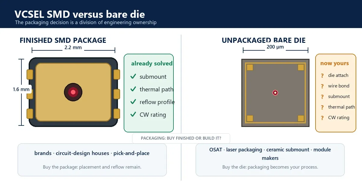
Buying VCSEL bare die instead of a finished SMD package is not really a price decision, and it is not a volume decision either. It comes down to whether any package can hit the emitter pitch your optics need, and only then to whether your line can own die attach and wire bonding. Work it in that order: calculate the pitch, check whether an SMD fits it, and ask about capability last. Most red light boards are settled before the third step.
Scope. This article covers emitter format and package selection. Optical dose validation, laser-safety classification, and finished-product certification sit outside it. Specifications quoted below come from the 660nm VCSEL SMD Series and Bare Die Series product data; confirm them against the applicable datasheet for the model you select, since figures are model-specific.
What you are actually buying
An SMD is a finished package. Someone has already chosen the submount, run the thermal path out to the pads, qualified a reflow profile, and characterized what came out. The 660nm VCSEL SMD series arrives as 2016, 2835, 3030, or 5730 parts in 5mW and 7mW classes. Your line places them and reflows them. The packaging problem was solved before the reel reached you, and you are paying for that.
A bare die is the emitter and nothing else. The 660nm VCSEL bare die series is supplied as unpackaged chips at 200μm scale in single, three, and six emitter configurations, for die attach, gold-wire bonding, and ceramic-submount assembly. Everything the SMD had already decided is now an open question you own.
That split maps onto who buys what. Brands and circuit-design houses running pick-and-place buy packages. OSAT providers, laser-packaging companies, ceramic-submount integrators, module makers, and lens and beam-shaping teams buy die. Neither is a more advanced version of the other. They are different jobs. Figure 1 summarizes what each format already includes and what it leaves open.
A qualified CW rating belongs to the finished assembly, not the die
One specification difference decides more projects than cost does, and it hides in the test conditions.
The 660nm SMD parts are rated CW or QCW depending on the model. The unpackaged die models are all specified under QCW only: 0.5ms pulse width, 1% duty cycle, at 25 °C.
That is not a limitation of the chip. It is a statement about what an unmounted die is. A bare die has no thermal path until you build one, so QCW is how you characterize a chip with nowhere to send its heat. Pulse it briefly, measure before the junction climbs, and you get an honest number for the emitter itself.
Read that as a sourcing fact and it gets blunt. A qualified CW rating is a claim about a finished assembly that someone else engineered and tested, not a property of the emitter inside it. Buy the VCSEL die and the rating does not transfer. It becomes a target you have to earn with your submount material, your die attach, your bond layout, and your own CW characterization. If your protocol needs continuous output, an SMD hands you a CW number and an unpackaged VCSEL hands you a project. It is the item most often left out when die gets costed against SMD.
Pitch decides the format, not volume
The received wisdom is that die is for high volume and SMD is for everyone else. In red light arrays that is usually wrong. What forces the decision is geometry.
A package has a size, and that size puts a floor under your emitter pitch. The 2016 is the smallest part in the 660nm SMD series at 2.2 × 1.6mm. Where that floor lands depends on the courtyard you design to. IPC-7351C recommends courtyard excess by density level: 0.12mm at Least, 0.25mm at Nominal, and 0.50mm at Most, and medical and high-reliability boards usually sit at the upper end. Add it on both sides and a square grid of 2016s bottoms out somewhere between about 2.4mm and 3.2mm center to center, or 1.8 to 2.6mm if you stagger the layout to use the short axis. No amount of volume moves those numbers. A 200μm die has no such floor, because the limit moves to your bond pads and your placement tooling.
Now bring in the beam. The 660nm SMD parts run 18° to 20° typical divergence, spot diameter goes as 2 × working distance × tan(divergence ÷ 2), and neighboring spots overlap only when the pitch is no larger than the spot. Other red parts differ, so run your own figure. The emitter pitch math is the same for both formats. What changes is whether a package can physically deliver the answer.
Working distance | Spot diameter (18°–20°) | Can an SMD grid overlap? |
|---|---|---|
20mm | ~6.3–7.1mm | Yes, any package at any density |
10mm | ~3.2–3.5mm | 2016 at Least or Nominal; Most at its limit |
7mm | ~2.2–2.5mm | 2016 at Least density only, and only just |
5mm | ~1.6–1.8mm | No, at any density |
3mm | ~1.0–1.1mm | No |
1mm | ~0.3–0.4mm | No |
Assumes the 2016 package, 18°–20° divergence, a square grid, and no secondary optics. A diffuser, a staggered layout, or a different part changes the answer.
<!-- Insert Figure 2 here: blog04-figure-2-working-distance.webp -->
As shown in Figure 2, at 10mm of standoff the spot is 3.2 to 3.5mm and a 2016 grid overlaps at Least or Nominal density, with Most right at its limit. Below 5mm the spot is under 1.8mm and no 2016 grid overlaps at any density, so there is nothing to negotiate: the options narrow to a VCSEL die on a custom submount, a diffuser, or a treated field made of dots. Between 5 and 10mm it comes down to which density level you design to and whether you stagger, and a Most-density medical layout is the one that runs out first. Panels, hoods, and most masks sit above the line. Contact wraps on an animal sit well below it, which is why that application keeps pulling teams toward custom packaging.
So the rule is unromantic. If a 2016 hits your pitch, buy the 2016. Volume does not change that, and a die-attach line bought to save money on parts you did not need to unpackage is a line you now have to feed.
Emitter count is a die-level lever
Where an unpackaged VCSEL does earn its place, emitter configuration turns into a design variable instead of a catalog choice. The 660nm die series gives three points to compare.
- 2mW, single emitter, 200μm × 200μm. 1.5–2.5mW at 10mA, 658nm – 660nm, 20° typical. One aperture, the simplest bond layout, and the tightest specified wavelength range of the three.
- 5mW, three emitters, 200μm × 200μm. 4–5mW at 10mA, 650nm – 670nm, 19° typical. Same footprint as the 2mW, more than double the output.
- 7mW, six emitters, 163μm × 185μm. 5–10mW with 7.5mW typical at 15mA, 655nm – 665nm, 20° typical. The smallest die and the highest output.
<!-- Insert Figure 3 here: blog04-figure-3-die-configurations.webp -->
Figure 3 compares the three side by side, and two things in it are worth stopping on. First, the 7mW die is the smallest one. It carries roughly five times the optical output per unit of die area that the 2mW carries, in a footprint about 25% smaller, at 15mA instead of 10mA. Heat leaves a die through its attach, and that die gives it the least area to leave through. Die attach quality matters most exactly where the die is smallest, which is the opposite of where teams tend to look for trouble.
Second, the specified wavelength ranges are not the same: 658nm – 660nm for the single emitter, 655nm – 665nm for the six, and 650nm – 670nm for the three. If unit-to-unit wavelength consistency is load-bearing for your device, that spread is a selection input rather than a footnote. We provide project-specific bin selection; start from what is specified.
All three produce the same symmetrical annular far field as the packaged parts, so the donut and the overlap problem come with you. The die does not fix beam shape. It changes how close together you are allowed to put the donuts.
What the cheaper-at-volume argument leaves out
The VCSEL die is cheaper than the package. That part is true, and it is where the analysis usually stops.
Underneath it sits a die bonder and a wire bonder, or a partner who has both. ESD-controlled handling. Incoming inspection, because you are buying chips now instead of tested packages. Submount and package NRE. Your own CW characterization, from the section above. And scrap, which is the quiet one: an SMD placed wrong can be desoldered and replaced, while a die bonded wrong is gone, and it usually takes the submount with it.
Bare die VCSELs can still win on total cost. They win after those are counted, and they mostly win for teams that were going to need custom packaging anyway. It rarely wins as a way to shave the bill of materials on a board a 2835 would have handled.
Four questions that settle it
- What pitch does your optical design need at your working distance? At 10mm or more a package fits at normal densities. Under 5mm, none in the series does at any density. In between, it depends on your courtyard density level.
- Do you need a submount, an array geometry, or an optic that sits at the die? If not, the package has already solved a problem you would be re-solving.
- Do you have die attach, wire bonding, and die-level ESD control, in-house or at a partner you trust? If not, this is not a purchasing decision, it is a capital plan.
- Can your program absorb scrap on a bonded die and its submount? SMD gives you rework. Die does not.
Questions one and two decide it. If both come back no, the answer is SMD however capable your line is. If either comes back yes, questions three and four only tell you whether to do the packaging yourself or have it done for you.
If you need die-level freedom but not die-level work
There is a third answer that gets skipped, and it fits more teams than either extreme.
When a team asks for a custom package, it is usually because one of three engineering constraints cannot be solved by a catalog part:
- Package size. The footprint puts a floor under the emitter pitch your optics need. That is the case the table above describes.
- Thermal path. The standard submount cannot move the heat your duty cycle and emitter count produce.
- Optical geometry. The array configuration, or an optic that has to sit at the die, is not something a placed part can give you.
If your design falls into one of those, custom packaging becomes an engineering answer rather than a purchasing preference. And it does not have to be your custom packaging. Package size, emitter layout, array configuration, wavelength tolerance, power binning, and divergence targets can be specified into a part that still arrives ready for pick-and-place. You keep placement. Someone else owns die attach, the thermal path, and the CW number. A custom development request is the route for that.
Before committing to any of it, most teams settle the question the same way, and it is not by reading a datasheet. They place a handful of parts on a real board at the real working distance and measure the field they actually get. Evaluation kits are one practical way to do that, in either format, and it is the cheap way to find out whether a standard package was going to work all along. That is the kind of project 1ONELASER typically supports.
One line does not move whichever way it lands. The emitter is a component. The finished-device manufacturer remains responsible for optical-dose validation, laser-safety classification, applicable photobiological risk assessment, product testing, labeling, and every claim on the box. Standards such as EN 60825-1 may be relevant to laser product classification depending on the finished product and jurisdiction. Buying die instead of packages moves the packaging work. It does not move that boundary.
FAQ
What is the difference between VCSEL SMD and bare die?
An SMD is a finished surface-mount package that your line places and reflows, with the submount, thermal path, and reflow profile already engineered. A bare die VCSEL is the unpackaged chip, supplied for die attach, gold-wire bonding, and ceramic-submount assembly. You take on the packaging work and gain control over pitch, submount, and geometry.
Is VCSEL bare die cheaper than SMD?
The part is cheaper. The decision is not. Bare die adds a die bonder and wire bonder, die-level ESD control, incoming inspection, submount NRE, your own CW characterization, and scrap on any die you bond wrong. It usually wins only for teams that needed custom packaging anyway.
Why is VCSEL bare die specified under QCW and not CW?
Because an unmounted die has no thermal path. QCW, here 0.5ms pulses at 1% duty cycle, characterizes the emitter before the junction heats. A packaged part carries a qualified CW rating because the assembly around it provides the heat path. Buy the VCSEL chip on its own and that rating becomes something your submount has to earn and your team has to verify.
When do I actually need bare die instead of SMD?
When package size blocks your emitter pitch, or when you need a submount, array geometry, or an optic at the die that no catalog part provides. As a rough line, a working distance of 10mm or more can be served by a 2016 at normal courtyard densities. Under roughly 5mm, no package in the series puts spots close enough to overlap at any density.
Which 660nm bare die should I choose?
By emitter count and die area. The 2mW single emitter on a 200μm square die has the simplest bond layout and the tightest specified wavelength range. The 5mW three-emitter fits more output into the same footprint. The 7mW six-emitter gives the highest output on the smallest die at 15mA, which also makes it the most demanding to attach and cool.
Does QCW data predict CW performance?
Not directly. QCW characterization at 0.5ms and 1% duty cycle measures the emitter before the junction heats, which is why it is the honest way to specify an unmounted die. Under CW the junction sits at a raised temperature, and optical output, center wavelength, and lifetime all move with it. How far they move depends on the submount and thermal path you build, so CW behavior has to be characterized on your own assembly rather than extrapolated from the QCW figure.
Does a smaller die always mean better optical density?
It means higher optical output per unit of die area, which is not the same as better. The 7mW six-emitter die carries roughly five times the optical output per mm² of the 2mW single emitter, in a footprint about 25% smaller. That density helps when board area is tight, but the heat still has to leave through the attach, and the smallest die gives it the least area to leave through. Density is a lever, not a free upgrade.
Can I get a custom SMD package instead of going to bare die?
Often, yes, and it is worth pricing before buying a bonder. Custom packaging is usually the answer to one of three constraints a catalog part cannot meet: package size blocking your pitch, a thermal path that will not carry your duty cycle, or an array geometry or optic that has to sit at the die. Package dimensions, emitter layout, array configuration, wavelength tolerance, and power bins can be specified into a part that still arrives ready for pick-and-place, which keeps die attach and the thermal path with the supplier.
References
- IPC-7351C, Generic Requirements for Surface Mount Design and Land Pattern Standard
- EN 60825-1, Safety of laser products